

- Abdullah Serdar Yonar
- Pier Andrea Francese
- et al.
- 2023
- ISSCC 2023
High-Speed I/O Links
Designing the next generation High-Speed I/O Links targeting low power consumption, low latency and small silicon area.
Overview
Data-centric workloads fuel the demand for interconnect technologies in which high-speed, low-latency and coherent data are transmitted and received efficiently across lossy and dispersive electrical and optical physical channels. The throughput (Gbps), efficiency (pJ/b) and latency (ns) of the data communication between CPUs, GPUs, FPGAs and emerging processing units, such as AI accelerators, and quantum-computers are at end the performance metrics that gate the overall performance and ultimately define the winning architecture of any physically distributed system. This project aims at demonstrating in the most advanced CMOS nodes data converters (DACs and ADCs) based links, analog front-ends comprising passive multi-tap coils for broadband on-die termination and ESDs, high-frequency continuous-time-linear equalizers (CTLEs), variable-gain-amplifiers (VGAs), clock generators as well as conventional wireline transmitter and receiver architectures targeting record low power consumption and latency and small silicon area.
The primary target applications are the next generation of high-speed I/Os for the IBM flagship processors deployed into the Z and P systems. The aggregate IO bandwidth and efficiency is a key premium differentiator in the market for the IBM systems that are heavily deployed in mission critical workloads in particular for transactions and associated data analysis and verifications. In parallel, new emerging computational systems for quantum computing (QC) operating at challenging cryogenic temperatures and for both artificial intelligence (AI) and machine learning (ML) applications are rapidly increasing their demand for dedicated IO technologies. The most common signaling format is two-levels NRZ and it is transitioning to multi-level signaling such as PAM4: More sophisticated constant envelop transmission (OFDM, discrete multitone) are expected to be deployed in the upcoming future.
Data converters for Digital Communications
The growing number of networked electrical/optical devices increases the demand for high-speed data transfer. Data center traffic grows due to emerging applications that imposes stringent requirements. Data intensive applications such as AI and machine learning further contributes to the need for high-speed data transfer across several domains. High speed serial links aggregate data rates must adapt to meet the future demand. The most effective solution for this is to increase the per-lane data rate as reflected in the requirements of various communication standards. On average, the data rate per pin doubles every four years for most of the wireline standards.
Modulation Formats beyond 100Gb/s – PAM4, PAM8 and OFDM
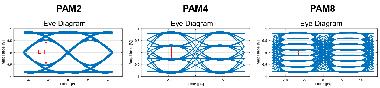
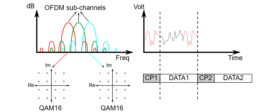
The data rate trend can be sustained through increasing the spectral efficiency of the signaling format. The emerging wireline standards proposes packing more bits per symbol which relaxes the bandwidth requirements of the links. For Pulse Amplitude Modulation (PAM) the data is encoded in the signal amplitude levels. Increasing the number of levels results in higher spectral efficiency. The eye diagram for PAM2, PAM4 and PAM8 are shown in Fig. 1. PAM4 is widely adopted for links supporting above 56Gb/s and PAM8 is being discussed as a candidate for the next generation links. OFDM is another strong candidate for the future links that employs sub-carriers distributed in the frequency domain which are modulated by parallel data as shown in Fig. 2. OFDM based links offers flexibility of optimizing each sub-channel and advanced equalization in digital domain. Higher order modulation techniques provide a way to increase the per-lane data rate however they lead to more complex TX-RX architectures.
Figure 1: PAM2, PAM4 and PAM8 eye diagrams.Figure 2: OFDM sub-channels and time domain waveform.DSP-based Link Architectures
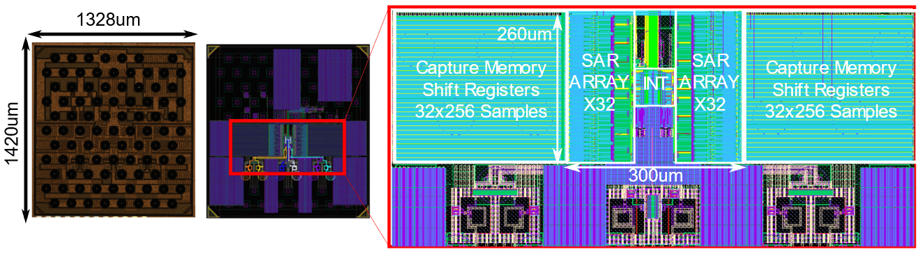
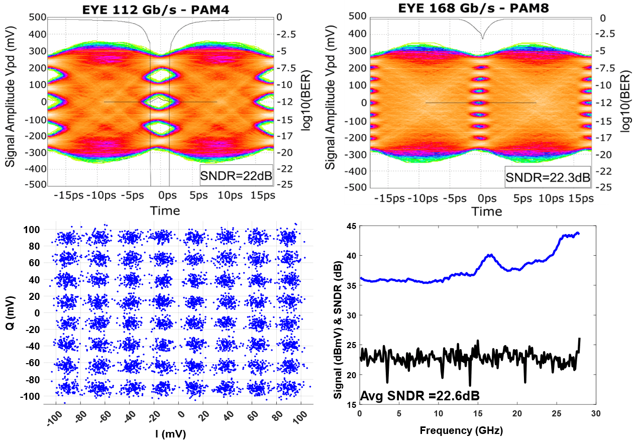
Spectrally efficiency modulation formats necessitate DAC- ADC-DSP based link architectures which can offer complex equalization strategies and signal detection techniques in digital domain. The heart of such wireline transceivers are the high-speed DACs and ADCs which mostly determines the power efficiency and the bit error rate. To reach tens of GS/s sampling speed the DACs, on one side, are implemented with fully custom sub-rate pre-drivers and serializers. The full-rate output drivers at the DAC output reach the highest switching speed offered by the technology in use. Multi-tap coils couple the DAC output signal into the physical channel with reliable ESD protection and termination in accordance with the standards. The ADCs, on the other side, contain sub-ADC arrays that operate in a time interleaved manner as illustrated in Fig. 3. This further complicates the design which requires the suppression of errors stemming from the time interleaving. Furthermore, the ADC must provide enough resolution to support the emerging signaling formats. The ADC-DSP based approach also provides flexibility in choosing the modulation format. In Fig. 3 we demonstrate experiments with PAM4 and PAM8 and in Fig. 4 with OFDM in which the received data is error free with forward error correction. The future links will demand even higher performance from the ADC. In IBM Research Zurich we work on advancing the existing architectures while moving forward with the emerging concepts that are tailored for the most recent CMOS nodes. Targeting the data rates above 100Gb/s, our work concentrates on achieving even higher speeds with the state-of-the-art figure of merits fused with innovative techniques.
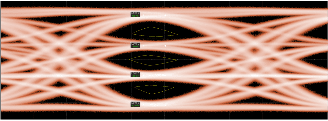
Figure 3: Layout details of a 64x time interleaved ADC. From An 8b DAC-Based SST TX Using Metal Gate Resistors with 1.4pJ/b Efficiency at 112Gb/s PAM-4 and 8-Tap FFE in 7nm CMOS, ISSCC 2021Figure 4: The eye diagrams for PAM4 and PAM8 and the constellation diagram for 64 QAM OFDM measured by the 56GS/s ADC. The results are error free with FEC. From An 8-bit 56GS/s 64x Time-Interleaved ADC with Bootstrapped Sampler and Class-AB Buffer in 4nm CMOS, VLSI Technology and Circuits 2022Publications
- A. Serdar Yonar
- Pier Andrea Francese
- et al.
- 2022
- VLSI Technology and Circuits 2022
- Marcel Kossel
- Vishal Khatri
- et al.
- 2021
- ISSCC 2021
- Abdullah Serdar Yonar
- Pier Andrea Francese
- et al.
- 2020
- IEEE SSC-L
- Yang You
- Glen Wiedemeier
- et al.
- 2020
- VLSI Circuits 2020
- Gain Kim
- Marcel Kossel
- et al.
- 2020
- IEEE JSSC
- Gain Kim
- Lukas Kull
- et al.
- 2019
- A-SSCC 2019
- Alessandro Cevrero
- Ilter Ozkaya
- et al.
- 2019
- ISSCC 2019