About
MODES is an EU Horizon 2020 Marie Skłodowska-Curie Individual Fellowship under grant agreement No. 704045. In this project we investigate direct epitaxial growth techniques for the monolithic integration of III–V material on silicon. We will explore the design and fabrication of passive and active photonic devices based on integrated III–V materials and their optical coupling Si-on-insulator waveguides.
The principal investigator is Stephan Wirths. MODES started in July 2016 and will run through June 2018. IBM Research – Zurich is the host institution.

Description
The microelectronics industry is facing a very serious challenge: traditional transistor scaling is approaching physical limitations, and the cost vs. performance gain is diminishing. Furthermore, the energy dissipated in interconnects of devices already accounts for more than 50% of the total energy used on a chip. This limits attainable clock speeds and fast data exchange between processors and memory. Optical communication is a very promising solution to address these interconnect problems, enabling a more energy efficient distribution of clock signals and of information between cores.
Although silicon (Si) is the ideal material for optical waveguides, it lacks the direct band gap required for optically active devices. Integrating compound semiconductors consisting of elements from group III and group V (III–V materials) for photonic devices directly on Si is obviously the most promising path to address these issues, but has not been demonstrated in an economically feasible way. This would enable large-scale optoelectronics integration hindered so far by coupling and overlay issues introduced by state-of-the-art III–V bonding on silicon.
The MODES project will develop and investigate a novel approach for self-aligned monolithic integration of active and passive III–V optoelectronic devices on a silicon platform. It focuses on optimizing GaAs- and InP-based III–V growth within customized oxide templates. Moreover, this research aims at designing and fabricating doped, defect-free III–V heterostructures for electrically-driven optoelectronic devices integrated on Si.
Three main objectives will be pursued:
- Growth and integration of III–V material with Si-on-insulator waveguides,
- Design and fabrication of passive and active photonic devices based on integrated III–V materials and Si waveguides,
- Optical and electrical characterization of the photonic components.
Materials integration
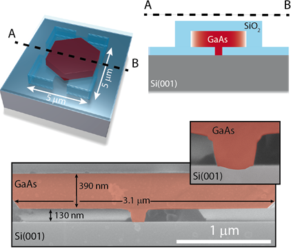
In the MODES project, we are exploiting Template Assisted Selective Epitaxy (TASE) for the monolithic integration of III–V materials on a silicon platform. This technology was invented at IBM [1] and has been employed for various electronic applications [2,3]. The core of the technique is to start the epitaxial growth from a Si surface small enough to allow only one nucleation point and use hollow oxide cavities up to the µm-size to guide the growth vertically and laterally. TASE provides a number of important advantages over many other growth techniques, e.g. we are able to grow on any crystalline orientation and even using amorphous Si [4], thus enabling novel innovative photonic device designs.
The challenge, however, consists of upscaling this integration technique from electronic (sub-100 nm) dimensions up to the µm or even millimeter scale for developing photonic components. In this context, we aim to integrate active and passive III–V photonic devices in close connection with Si waveguides.
Local III–V integration for active photonic devices is essential to enable fully integrated photonic circuits with hundreds or thousands of active components.

Publications
- Schmid, H.; Borg, M.; Moselund, K.; Gignac, L.; Breslin, C. M.; Bruley, J.; Cutaia, D. & Riel, H., “Template-assisted selective epitaxy of III-V nanoscale devices for co-planar heterogeneous integration with Si,” Applied Physics Letters 106, 233101, 2015.
- Czornomaz, L.; Uccelli, E.; Sousa, M.; Deshpande, V.; Djara, V.; Caimi, D.; Rossell, M. D.; Erni, R. & Fompeyrine, J., “Confined Epitaxial Lateral Overgrowth (CELO): A novel concept for scalable integration of CMOS-compatible InGaAs-on-insulator MOSFETs on large-area Si substrates,” Symposium on VLSI Technology, pp. T172 - T173, 2015.
- Cutaia, D.; Moselund, K. E.; Schmid, H.; Borg, M.; Olziersky, A. & Riel, H.,“Complementary III-V Heterojunction Lateral NW Tunnel FET Technology on Si,” Symposium on VLSI Technology, 2016.
- Borg, M.; Schmid, H.; Moselund, K. E.; Signorello, G.; Gignac, L.; Bruley, J.; Breslin, C.; Kanungo, P. D.; Werner, P. & Riel, H., “Vertical III-V Nanowire Device Integration on Si(100),” Nano Letters 14, 1914-1920, 2014.
