Advanced interconnects
Interfaces within electronic packages are typical sources of losses in transport processes. Therefore, a main challenge is to explore materials and processes to advance interconnects in general. We pursue two novel concepts taking advantage of nanoparticles to improve electrical and thermal transport to and from an integrated circuit die.
All-copper interconnects
“Our main challenge is to explore materials and processes to advance interconnects in general. We pursue two novel concepts taking advantage of nanoparticles to improve electrical and thermal transport to and from an integrated circuit die.”
—IBM scientist Luca Del Carro
Currently, microprocessors are connected to printed-circuit boards (PCB) by several 10,000s of solder balls, which are arranged in a regular grid on the underside of the chip. As much as 80% of the electrical interconnects are occupied for provisioning up to 300 amperes of current, whereas only 20% are left for the main purpose of signaling.
The solder ball interconnect technology was invented by IBM engineers in the 1960s, resulting in the still widely used flip chip technology. A chip with solder balls is placed onto a PCB and both components are transferred to an oven. The solder melts above 230°C and instantly wets the pads of the PCB. During cooling, the solder solidifies to form the electrical contact. A challenge is that voids form in the solder interconnects at high current densities, which can lead to system failures. The voids are a consequence of the passing “electron wind”, causing material transport in the direction of the current flow.
An alternative interconnect material to solder is copper, a material already used for electrical wires for most chips and PCBs. Copper is about ten times more resistant against electron wind, resulting in what is termed electromigration. Currently, the industry is reducing solder amounts, which means that Cu-pillar interconnects have lower pitches and higher current carrying capabilities (Figure 1).
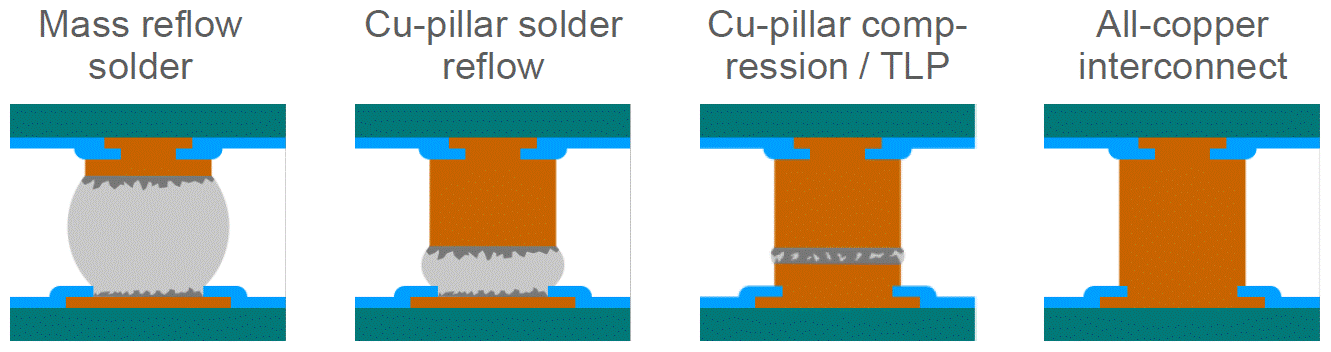
Figure 1: Electrical interconnect roadmap, from solder to all-copper interconnects.
The ultimate goal is to achieve interconnects with copper only in order to mitigate negative effects promoted by solder and any brittle intermetallic compound [1]. The challenge is the physical limitation of the high melting temperature of copper (1085°C).
To achieve all-copper interconnects, a paste containing copper micro and nanoparticles is used. Firstly, this paste is smeared out with a technique called “doctor blading” to yield a uniform Cu-paste film. Secondly, the Cu paste is transferred to Cu pillars of a microprocessor chip by dipping. Subsequently, the chip is aligned and placed onto pads of a PCB. The final joints are achieved by annealing at 160°C under no pressure in a formic-acid atmosphere [2]. This is possible because nanoparticles have a very large surface compared to their volume and hence the diffusion of Cu atoms is promoted to form metallic contacts.
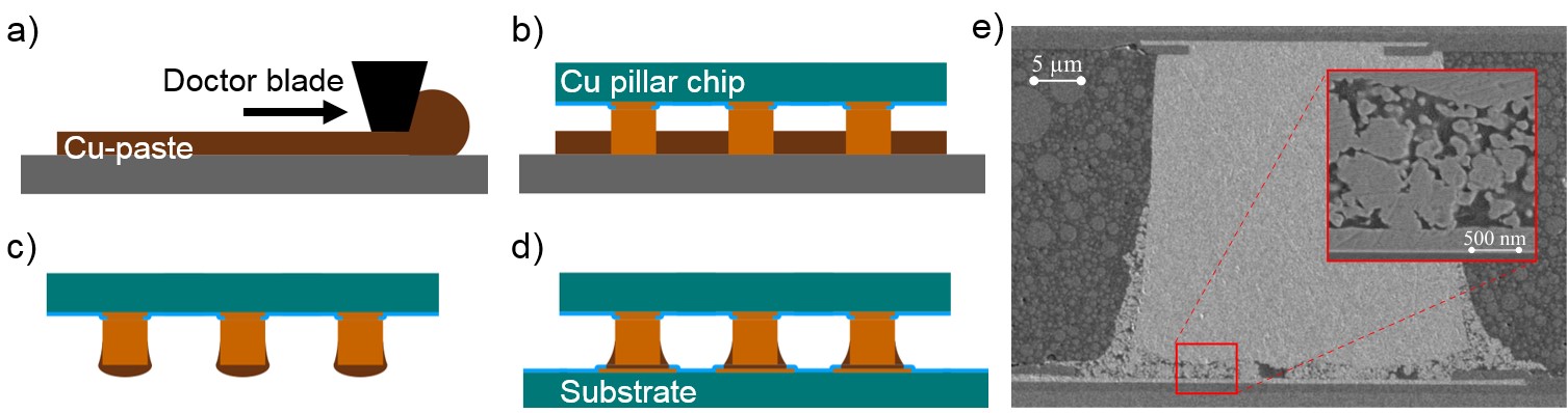
Figure 2: All-copper interconnect process flow: a) Copper paste film formation, b) copper pillar dipping, c) die alignment, d) joining by sintering. e) Scanning electron micrograph of an all-copper interconnect.
Percolating thermal underfill
A major barrier for heat-removal within integrated circuit stacks is the solder ball array interface between dies when traditional packaging materials are used. The space between the solder balls is traditionally filled with a capillary underfill (CU), composed of silica fillers dispersed in an adhesive matrix in order to mitigate mechanical stress concentrations and thus to improve mechanical reliability. Thermal capillary underfills, premixed with thermal filler particles (e.g. alumina substituting silica), are intended to improve the thermal conductivity of the underfill layer, albeit with modest success due to the limited particle fill fractions.
In percolating thermal underfills (PTUs) densely packed micron-sized dielectric particles fill the open space caused by the electrical interconnects between individual chips within a stack [3]. The composite material benefits from superior thermal conductivity if the microparticle loadings are above the percolation threshold and the particles form continuous networks. Percolation is achieved by the formation of particle beds during centrifugation. Enhanced thermal particle-to-particle contact is achieved by the self-assembly of thermally conductive nanoparticles through capillary bridging during solvent evaporation (Movie 1), resulting in quasi-areal contacts, called necks, between the filler particles (Figure 3a) [4]. The sequential process is completed by adhesive backfilling to achieve mechanical integrity of the thermally conductive underfill.
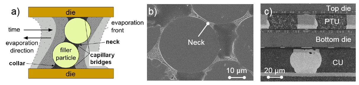
Figure 3: Cross section a) schematic depicting neck formation by capillary bridging and scanning electron micrograph of b) resulting bi-modal necks between filler particles and c) a 3D chip stack with percolating underfill.
An effective thermal conductivity of up to 2.8 W m−1 K−1 has been measured for such neck-based thermal underfills, compared to 0.7 W m−1 K−1 for thermal capillary underfills. Different nanoparticle sizes and distributions yield different neck morphologies. It has been demonstrated that the use of a mixture of two particle sizes yields the best results concerning packing density and defect prevention, which maximizes the effective layer thermal conductivity (Figure 3b). The percolating thermal underfill was also applied successfully to 3D chip stacks (Figure 3c).
References
[1] J. Zuercher, T. Brunschwiler, et al., “Nanoparticle assembly and sintering towards all-copper flip chip interconnects,” Proceedings of ECTC, San Diego, 2015.
[2] J. Zuercher, T. Brunschwiler, et al., “All-copper flip chip interconnects by pressureless and low temperature nanoparticle sintering,” Proceedings of ECTC, Las Vegas, 2016.
[3] T. Brunschwiler, J. Zuercher, S. Zimmmermann, B. Burg, G. Schlottig, R. Straessle, et al., “Review on percolating and neck-based underfills for three-dimensional chip stacks,” Journal of Microelectronics and Electronic Packaging, 138(4), 2016.
[4] J. Zürcher, X. Chen, B. R. Burg, T. Brunschwiler, S. Zimmermann, et al., “Enhanced percolating thermal underfills achieved by means of nanoparticle bridging necks,” IEEE Transactions on Components, Packaging and Manufacturing Technology, PP(99), 1-11, 2016.
Ask the expert

Thomas Brunschwiler
IBM Research scientist
Related projects


HyperConnect
Functional joining of dissimilar materials using directed self-assembly of nanoparticles by capillary-bridging