Modern information technologies rely on three key components:
1 A dense and mobile network of nodes to collect and preprocess data
· Smartphones, Internet of things
2 An efficient, broadband infrastructure to transmit data
3 A de-materialized space for high-performance processing of data
· Cloud infrastructure
At the beginning and at the end of the chain, the tradeoff between power and performance becomes increasingly challenging. This translates into reduced battery lifetime and major challenges regarding the cooling of datacenters.
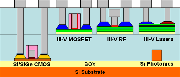
Post-CMOS technology
After decades of geometrical scaling, the power–performance–density tradeoff of CMOS technology can only be maintained if new materials are introduced. High-κ dielectrics have allowed designers to maintain the supply voltage, while keeping the parasitic power low related to gate leakage. High-mobility channels aim to reduce parasitic power induced by source–to–drain leakage. They will allow the supply voltage to be reduced, while maintaining a large drain current and therefore a high performance level. Owing to the mismatch in electron and hole mobilities in compound semiconductors, a co-integrated InGaAs/SiGe technology is the only approach available to make progress in CMOS technology.
“Our team was the first to demonstrate a hybrid InGaAs/SiGe CMOS technology on a silicon substrate.”
—Lukas Czornomaz
IBM Research scientist
Introducing high-mobility channel materials into an advanced CMOS technology can improve the power–performance tradeoff comparable to what conventional Si CMOS could potentially offer with 2–3 scaling nodes.
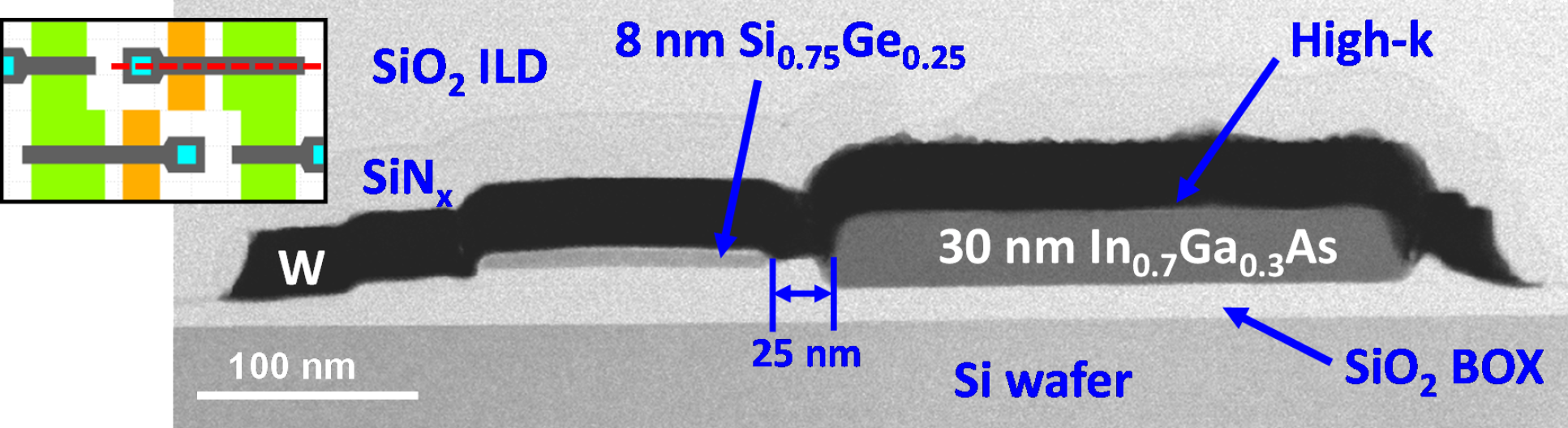
For many years, the technological bottleneck has been to demonstrate a path that enables simultaneously the growth of defect-free InGaAs, the fabrication of high-performance InGaAs field-effect transistors “on-insulator” co-processing them with SiGe devices, all on a silicon substrate and compatible with standard CMOS design environments.
Hybrid InGaAs/SiGe
With more than ten years of expertise in this field, our team has developed unique methodologies to integrate InGaAs on large-scale Si substrates, to build CMOS-compatible transistors and optimize their performance, and to demonstrate hybrid CMOS circuits and evaluate their impact on future CMOS technology nodes.
Our team was the first to demonstrate a hybrid InGaAs/SiGe CMOS technology on a Si substrate, for which we use processes suitable for high-volume manufacturing on 300-mm wafers. Based on selective epitaxy, our approach yielded functional inverters and dense arrays of 6T–SRAMs, the basic blocks of digital CMOS circuits. This work — the first of a kind — was recently disclosed at the latest VLSI Technology conference. It concludes a series of key demonstrations for InGaAs/SiGe CMOS, which have been reported in numerous contributions and highlights for the past five years at IEDM meetings and VLSI Technology Symposia.
3D monolithic integration
Another strong trend in the semiconductor industry is to enhance density scaling by going into the third dimension. Three-dimensional monolithic integration allows layers of devices or functions to be stacked on top of each other, thus increasing the density and functionality of the chip while reducing power losses from wire lengths and other parasitics. It also offers unique advantages to integrate high-mobility materials owing to their intrinsically low processing thermal budget.
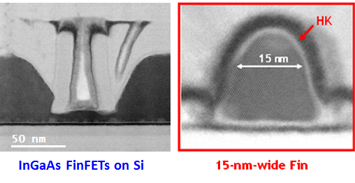
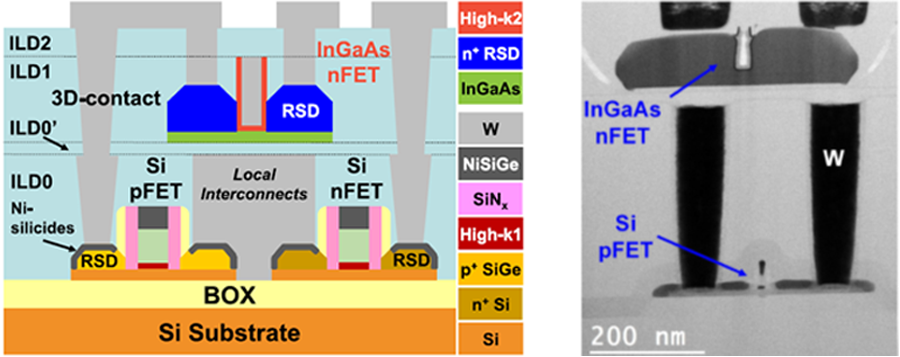
Our team has succeeded in showing that independently optimized layers of InGaAs FinFETs and SiGe FinFETs can be stacked without the top-layer processing having an impact on the bottom-layer performance to demonstrate functional inverters. This technology achievement will allow RF-over-CMOS applications as well as III–V photonic devices integrated with Si photonics and CMOS.
The demonstration of scaled InGaAs/SiGe hybrid CMOS circuits has profound consequences for manufacturing technologies. It proves that processes, metrology, and best practices for environments as different as silicon and III–V process lines can indeed be merged into a single processing environment.
Beyond digital applications, this paves the way to the development of fabrications designed for hybrid technologies, be they for wireless, power or optical technologies. These tremendous developments could represent a paradigm change for both CMOS and III–V industries.
Ask the experts


Related EU projects

COMPOSE3
Compound Semiconductors for 3D integration

III–V–MOS
Technology CAD for III–V Semiconductor-based MOSFETs

Insight
Integration of III–V Nanowire Semiconductors for next Generation High Performance CMOS SOC Technologies


Publications
[1] “DC and RF characterization of InGaAs replacement metal gate (RMG) nFETs on SiGe-OI FinFETs fabricated by 3D monolithic integration”
V. Deshpande et al.
Solid State Electronics, 128, 87–91, 2017.
[2] “First Integration of InGaAs/SiGe Channels into Dense SRAM Arrays with sub-0.45 m2 Cell Size Fabricated Using Standard CMOS Processes”
L. Czornomaz et al.
In Proc. Symposium on VLSI Technology, p. T9–2, 2016.
[3] “Confined Epitaxial Lateral Overgrowth (CELO): A Novel Concept for Scalable Integration of CMOS-compatible InGaAs-on-insulator MOSFETs on Large-Area Si Substrates”
L. Czornomaz et al.
In Proc. Symposium onVLSI Technology, pp. T172–T173, 2015.
[4] “Advanced 3D Monolithic Hybrid CMOS with Sub-50 nm Gate Inverters Featuring Replacement Metal Gate (RMG)-InGaAs nFETs on SiGe-OI Fin pFETs”
V. Deshpande et al.
In Proc. IEEE International Electron Devices Meeting (IEDM), pp. 8.8.1–8.8.4, 2015.
[5] “An InGaAs on Si platform for CMOS with 200 mm InGaAs-OI substrate, gate-first, replacement gate planar and FinFETs down to 120 nm contact pitch”
V. Djara et al.
In Proc. Symposium on VLSI Technology, pp. T176–T177, 2015.
[6] “CMOS-compatible Replacement Metal Gate InGaAs-OI FinFET With ION = 156 µA/µm at VDD = 0.5 V and IOFF = 100 nA/µm”
V. Djara et al.
Electron Device Letters, 37(2), 169–172, 2016.
[7] “Towards large size substrates for III-V co-integration made by direct wafer bonding on Si”
N. Daix et al.
Applied Physics Letters – Materials, 2(8), 086104, 2014.
[8] “Co-integration of InGaAs n- and SiGe p-MOSFETs into digital CMOS circuits using hybrid dual-channel ETXOI substrates”
L. Czornomaz et al.
In Proc. IEEE International Electron Devices Meeting (IEDM), pp. 2.8.1–2.8.4, 2013.
[9] “Scalability of ultra-thin-body and BOX InGaAs MOSFETs on silicon”
L. Czornomaz et al.
In Proc. European Solid-State Device Research Conference (ESSDERC), pp. 143–146, 2013.
[10] “An integration path for gate-first UTB III-V-on-insulator MOSFETs with silicon, using direct wafer bonding and donor wafer recycling”
L. Czornomaz et al.
In Proc. IEEE International Electron Devices Meeting (IEDM), p. 23.4.1, 2012.
[11] “CMOS compatible self-aligned S/D regions for implant-free InGaAs MOSFETs”
L. Czornomaz et al.
Solid-State Electronics, 74, 71–76, 2012.
[12] “Thermally stable, sub-nanometer equivalent oxide thickness gate stack for gate-first In0.53Ga0.47As metal-oxide-semiconductor field-effect-transistors”
M. E. Kazzi et al.
Applied Physics Letters, 100(6), 063505, Feb. 2012.
[13] “1.2 nm capacitance equivalent thickness gate stacks on Si-passivated GaAs”
M. El Kazzi et al.
Microelectronic Engineering, 88(7), 1066–1069, 2011.