Our research
III–V materials provide several advantages over silicon. They have lower effective masses, higher mobilities and a direct bandgap, which renders them more suitable for both photonic and tunneling devices. Silicon has been and will continue to be the semiconductor of choice for the electronics industry. Si is abundant, low cost, robust and provides an ideal passivation in terms of the high-quality SiO2 oxide.
In order to combine the best of both worlds, III–V integration on Si is of great technical as well as economic interest and has been pursued for many years. A visionary example of embedded device integration is illustrated schematically in Fig. 1. Close proximity of III–V devices with Si-based circuits can improve system performance or even enable new application areas. It is also anticipated that system fabrication costs will be significantly lower than discrete chip packaging approaches.
Accordingly, many different approaches towards this goal have been developed, ranging from the mechanical transfer of III–V device layers to a Si wafer as well as growing epitaxial films directly on Si. One of the key challenges to epitaxial approaches is to overcome material defects stemming from the crystal lattice mismatch with Si. Figure 2 shows the lattice constant and bandgap of various important III–V compounds, including Si.
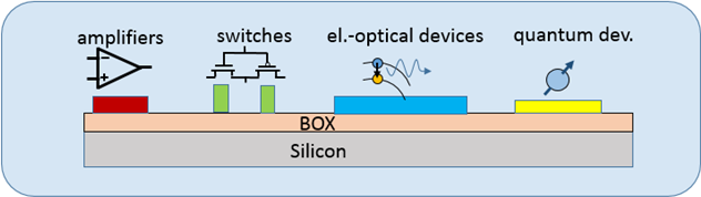
Figure 1. Schematic illustration of the various application spaces of III–V materials and devices on Si.
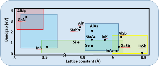
Figure 2. Bandgap versus lattice constant of several semiconductors of technological relevance. The greater the difference in lattice constant between two materials, the more challenging their co-integration.
Template-assisted selective epitaxy (TASE)
We have developed an epitaxial growth method to deposit III–V materials on Si, which results in good material quality and is compatible with CMOS processes.
We have deposited various III–V compounds on Si and processed the nanowires or platelets in state-of-the-art field effect transistors (FETs), heterojunction tunnel FETs.
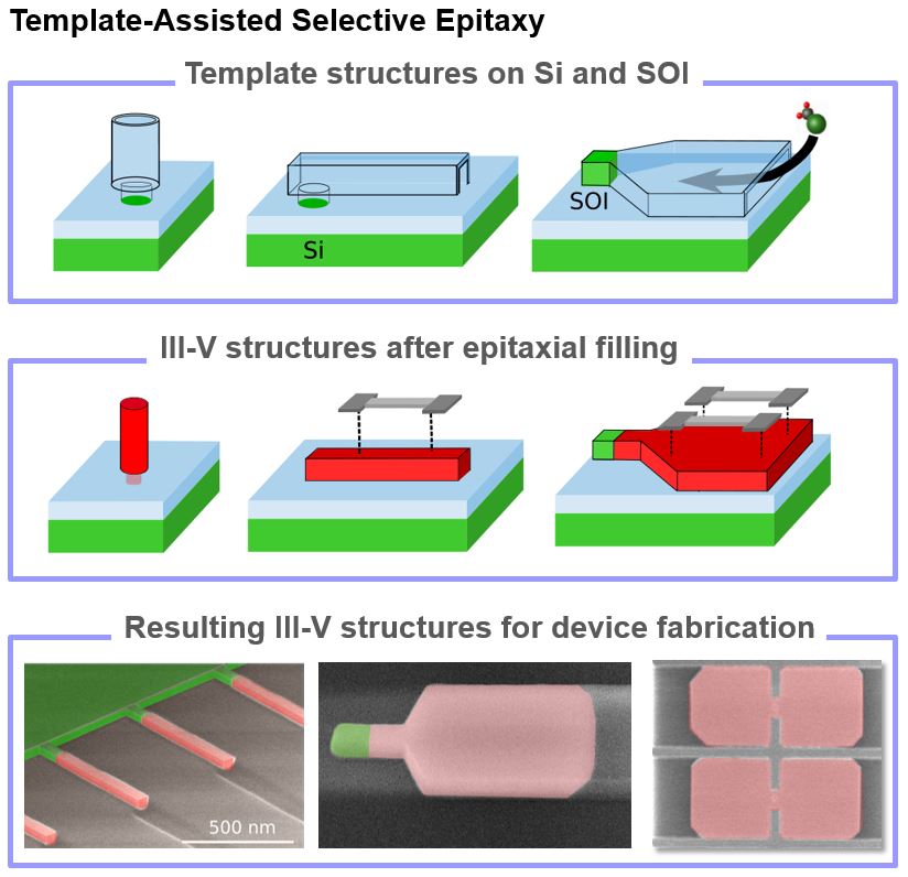
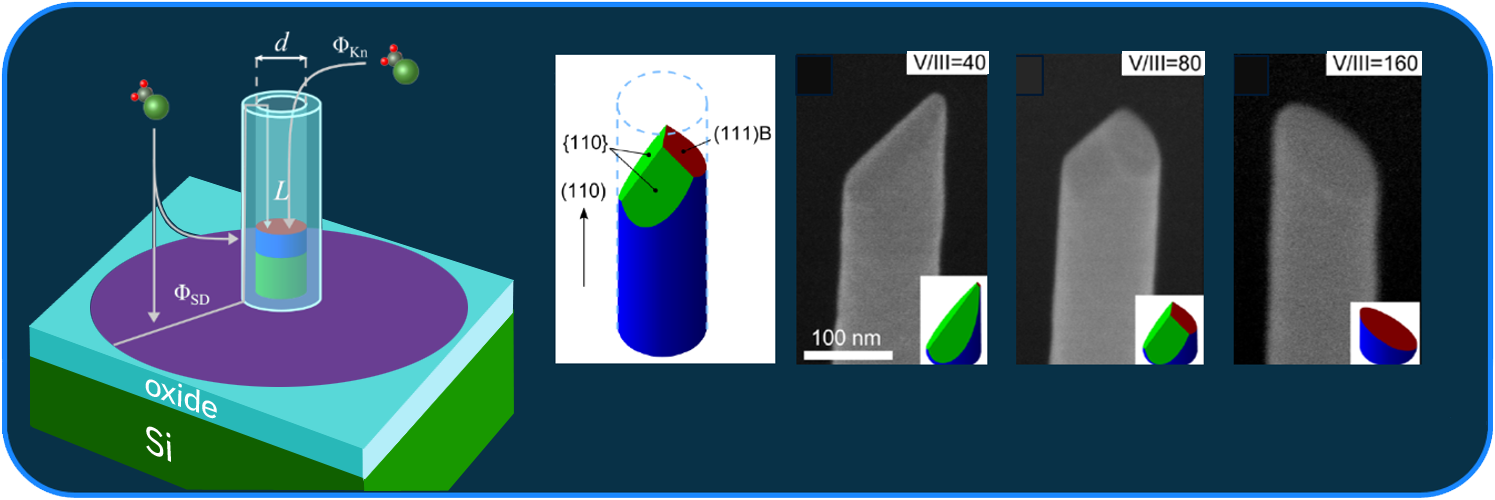
With the template-assisted selective epitaxy (TASE) method, the III–V material is deposited selectively on a small (Si) seed crystal, which can be located on a Si or silicon-on-insulator (SOI) wafer. Continuing from this nucleation step, the III–V crystal grows further and expands into the predefined template until it fills the entire cavity.
Growth dynamics
A good understanding of the epitaxy process is essential for enabling high-performance materials and devices as well as for developing strategies for cointegration.
We have previously studied the growth of “bottom-up” III–V nanowires using selective area growth (SAG) in oxide mask openings. Whereas this SAG yields NWs free from detrimental structural defects, attainable NW geometries, surface and growth orientation are very limited because of surface diffusion and reaction kinetics of the precursor molecules and nanowire-free surface energies. This has inspired us to develop an alternative method based on epitaxy in templates that can alleviate many of the above constraints.
We started with the initial demonstration of III–V heterostructures on Si(111) in a SiO2 template and have progressed to much more complex structures, devices and integration schemes. We found that the crystal growth in the template follows classical crystal growth physics. After initial nucleation, favorable growth planes develop and, depending on the growth conditions, prevail throughout the filling process.
The material delivery from the gas phase mixture into the template differs from classical selective-area growth or bottom-up nanowire growth processes because of the long surface diffusion path on the template and very small exposed III–V surface.
Molecular transport into a template (left). Schematic and corresponding SEM images of InAs crystal facet formation during MOCVD.
From “Observation of Twin-free GaAs Nanowire Growth Using Template-Assisted Selective Epitaxy,”
M. Knoedler et al.,
Crystal Growth & Design 17(12), 6297–6302, 2017.
Crystal quality
The formation of crystal defects is one of the key challenges in CMOS compatible III–V integration due to its effect on reliability and device performance. Whereas TASE avoids defects such as threading dislocations and antiphase boundaries, planar defectsare commonly observed in our structures. Thus, a profound understanding of the growth dynamics is required to control the crystal stacking and prevent unintended zinc-blende-wurtzite (ZB-WZ) intermixing.
We investigated the crystal quality of TASE-grown GaAs NWs dependent on growth conditions such as temperature and V/III ratio. NWs can be categorized according to the obtained growth facets, which typically consist of a single(110) plane or a combination of (110) planes together with a (111)B plane. The former type is found to grow without the formation of planar defects, resulting in a pure ZB crystal. NWs exhibiting (111)B facets typically show a large number of stacking faults independent of the growth conditions.
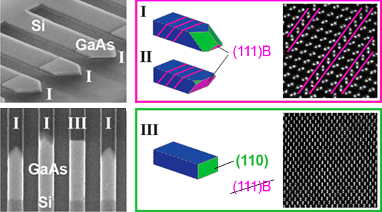
Growth facet formation in TASE. A single (110) growth front results in defect-free material.
Bonding
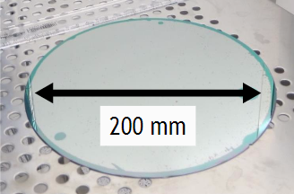
Direct wafer bonding is used to transfer thin layers of III–V onto silicon substrates as the industry is currently doing to build silicon-on-insulator (SOI) substrates. The required InGaAs layer is grown on a donor substrate, which is then bonded via an oxide to a target silicon substrate. The thin III–V layer is then released from the donor wafer, yielding a III–V-on-insulator structure on Si.
The donor wafer can be recycled in order to maintain the cost efficiency of this process. Having a very thin III–V channel on an insulator is the ideal structure to maintain good electrostatic control of the gate over the channel at short gate lengths. It also efficiently cuts leakage currents from source to drain. In addition, it enables the use of the back-biasing technique, which permits the transistor operation to be adjusted dynamically to make it either faster or more power-efficient. All these arguments are strong reasons why III–V-on-insulator structures might be the preferred option when addressing mobile applications.
We have mastered this technique and demonstrated that it can be scaled to large-size III–V-on-insulator on Si substrates. By using an epitaxial III–V on Si donor wafer, we can apply it to pre-processed CMOS wafers in order to stack several layers of active components in a 3D monolithic fashion. We have used this technique for the first-of-a-kind demonstration of an InGaAs/SiGe CMOS technology on Si. We are currently also exploiting this for the fabrication of active silicon photonics.
Furthermore, we have extended this technique to many other III–V materials beyond InGaAs as well as other non-III–V materials such as crystalline oxides. Among other things, we can use this technique to integrate InAs or GaSb on Si for further development of low-power logic circuits, GaP on Si for quantum opto-mechanics applications, or even barium–titanate on SOI for photonics applications.
InGaAs-on-insulator on Si.
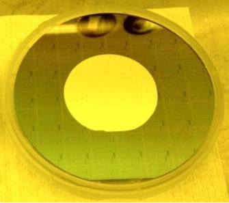
20-nm InGaAs transferred on CMOS wafer for 3D circuits.
Ask the experts


Daniele Caimi
IBM Research senior engineer


Publications
“Exploring the Size Limitations of Wurtzite III–V Film Growth,”
P. Staudinger et al.
Nano Lett. 20(1), 686–693, 2020.
“Wurtzite InP Microdisks: from Epitaxy to Room-Temperature Lasing,”
P. Staudinger et al.
arXiv:2004.10677, 2020.
“Concurrent Zinc-Blende and Wurtzite Film Formation by Selection of Confined Growth Planes,”
P. Staudinger et al.
Nano Lett. 18(12), 7856–7862, 2018.
“Monolithic Integration of III -V on silicon for photonic and electronic applications,”
S. Mauthe et al.,
In Proc. Device Research Conference 1-2, 2018.
“Monolithically integrated InGaAs microdisk lasers on silicon using template-assisted selective epitaxy,”
S. Mauthe et al.,
In Proc. SPIE 10672, Nanophotonics VII, 106722U, 2018.
“Room-Temperature Lasing from Monolithically Integrated GaAs Microdisks on Silicon,”
S. Wirths et al.,
ACS Nano 12(3), 2169-2175, 2018. DOI: (open access)
“Monolithic integration of III-V nanostructures for electronic and photonic applications,”
B. Mayer et al.,
In Proc. SPIE 10349, Low-Dimensional Materials and Devices, 103490L, 2017.
“Microcavity III-V lasers monolithically grown on silicon,”
B. Mayer et al.,
In Proc. SPIE 10540, Quantum Sensing and Nano Electronics and Photonics XV, 105401D, 2018.
“DC and RF characterization of InGaAs replacement metal gate (RMG) nFETs on SiGe–OI FinFETs fabricated by 3D monolithic integration,”
V. Deshpande et al.,
Solid State Electronics 128, 87–91, 2017.
“Observation of Twin-free GaAs Nanowire Growth Using Template-Assisted Selective Epitaxy,”
M. Knoedler et al.,
Crystal Growth & Design 17(12), 6297–6302, 2017.
“First Integration of InGaAs/SiGe Channels into Dense SRAM Arrays with sub-0.45 m2 Cell Size Fabricated Using Standard CMOS Processes,”
L. Czornomaz et al.,
In Proc. Symposium on VLSI Technology, p. T9-2, 2016.
“Local Thermometry of Self-heated Nanoscale Devices (Invited),”
F. Menges et al.,
In Proc. IEEE International Electron Devices Meeting (IEDM), 2016.
“Mechanisms of template-assisted selective epitaxy of InAs nanowires on Si,”
M. Borg et al.,
J. Appl. Phys. 117(14) 144303, 2015.
“Confined Epitaxial Lateral Overgrowth (CELO): A Novel Concept for Scalable Integration of CMOS-compatible InGaAs-on-insulator MOSFETs on Large-Area Si Substrates,”
L. Czornomaz et al.,
In Proc. Symposium on VLSI Technology, pp. T172–T173, 2015.
“Template-assisted selective epitaxy of III–V nanoscale devices for co-planar heterogeneous integration with Si,”
H. Schmid et al.,
Appl. Phys. Lett. 106, 233101, 2015.
“An InGaAs on Si platform for CMOS with 200 mm InGaAs–OI substrate, gate-first, replacement gate planar and FinFETs down to 120 nm contact pitch,”
V. Djara et al.,
In Proc. Symposium on VLSI Technology, pp. T176–T177, 2015.
“Advanced 3D Monolithic Hybrid CMOS with Sub-50 nm Gate Inverters Featuring Replacement Metal Gate (RMG)–InGaAs nFETs on SiGe–OI Fin pFETs,”
V. Deshpande et al.,
In Proc. IEEE International Electron Devices Meeting (IEDM), pp. 8.8.1–8.8.4, 2015.
N. Daix et al.,
“Towards large size substrates for III-V co-integration made by direct wafer bonding on Si,”
Appl. Phys. Lett. – Materials 2(8), 086104, 2014.
“Scalability of ultra-thin-body and BOX InGaAs MOSFETs on silicon,”
L. Czornomaz et al.,
In Proc. European Solid-State Device Research Conference (ESSDERC), pp. 143–146, 2013.
“Co-integration of InGaAs n-and SiGe p-MOSFETs into digital CMOS circuits using hybrid dual-channel ETXOI substrates,”
L. Czornomaz et al.,
In Proc. IEEE International Electron Devices Meeting (IEDM), pp. 2.8.1–2.8.4, 2013.
“InAs nanowire growth on oxide-masked 〈111〉 silicon,”
M.T. Björk et al.,
J. Crystal Growth 344(1) 31-37, 2012.
“An integration path for gate-first UTB III–V-on-insulator MOSFETs with silicon, using direct wafer bonding and donor wafer recycling,”
L. Czornomaz et al.,
In Proc. IEEE International Electron Devices Meeting (IEDM), 23.4.1, 2012.