Overview
 We are investigating ferromagnetism at the limit of today’s technology and beyond.
Magnetic anisotropy, domain configuration and domain wall properties are considered in systems when film thickness and lateral dimensions shrink.
We consider ways of controlling these magnetic parameters by structural modifications, which consist of well-defined steps and voids of geometrical or chemical origin, or of lithographically fabricated elements of various sizes and shapes.
Using such an approach, we are acquiring a better understanding of technologically relevant magnetic devices that necessarily deviate from an ideally flat surface.


Spin-polarized SEM
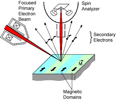
Spin-polarized scanning electron microscopy (spin-SEM or SEMPA) is an efficient technique to image the magnetization distribution at surfaces and in thin films.
An unpolarized electron beam, focused by electromagnetic lenses, scans across the ferromagnetic surface. At each scanned position, spin-polarized secondary electrons are created near the surface, emitted into vacuum and transferred to the spin analyzer by electrostatic lenses. There the electrons are scattered at a gold foil into preferential directions depending on their spin. A pair of detectors counts the electrons with “up” and those with “down” spin. The spin polarization of the emitted secondary electrons is a measure of the surface magnetization. The total number of electrons yields the surface topography map. In our setup [1-3], typical beam energies are 2 to 10 keV with a beam current of 0.1 to 1 nA.
This technique is able to image the magnetization of specimens with thicknesses down to a single atomic layer and a very high spatial resolution of better than 10 nm. Thus very detailed magnetization maps can be acquired.
Two magnetization components can be imaged simultaneously because the spin analyzer comprises two detector pairs. A spin rotator based on the Wien-filter principle [4] allows us to choose which magnetization components are imaged simultaneously, either the out-of-plane and one in-plane component, or the two in-plane components.
Magnetic nanostructures
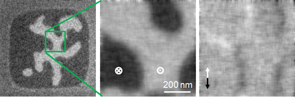
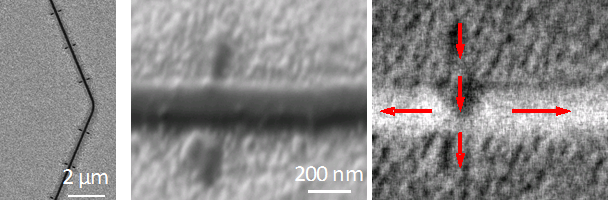
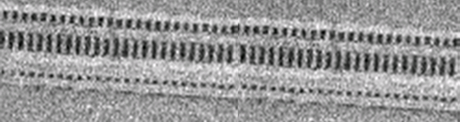
We image domain and domain walls in ferromagnetic nanostructures, which are fabricated by electron-beam lithography methods or by nanostenciling through membrane masks.
In these magnetic elements, we explore domain patterns and domain walls including their profiles and pinning behavior.
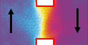
Bloch walls as narrow as 10 nm are imaged in perpendicularly magnetized structures, whereas Néel walls (transverse or vortex) are present in in-plane magnetized ultrathin elements.
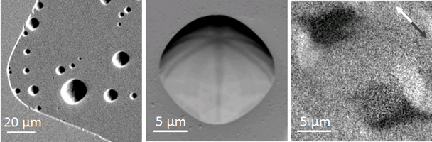
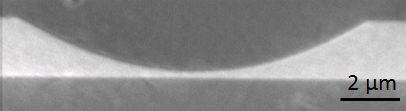
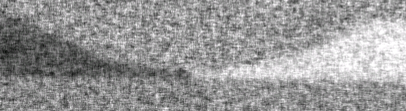
We create free-standing ultrathin ferromagnetic structures by bombarding magnetic films by noble gas ion beams [5]. Depending on the beam energy, this sputtering process can cause remarkable changes in sample topography.
In particular, blisters are created, which are hollow protrusions in which the ultrathin epitaxial Fe film is delaminated from the GaAs(001) substrate.
Starting from a homogeneously magnetized film, magnetic domains form at the blister rim because of elastic strain at the edge.
Domain-wall motion
The current-driven motion of domain walls is a key ingredient of several new concepts of novel magnetic memory and logic devices. Rather than moving walls by magnetic fields, it is the transfer of spin from the conduction electrons to the magnetization which drives the wall.
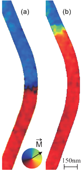
We have studied the propagation of domain walls in in-plane magnetized nanowires of FeNi and epitaxial Fe as well as in bilayer wires. Domain walls can be made to change their type from vortex to transverse [6,7] or exhibit symmetry-breaking properties [8]. In wider wires, domain walls are complex objects in which individual parts exhibit their own dynamics, as we have shown in a time-resolved Kerr microscopy study [9].
Our experiments are complemented by micromagnetic simulations within the OOMMF framework [10], for which we have implemented a spin-transfer torque extension [11], which is freely available for download here.
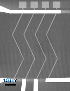
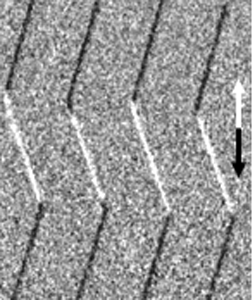
Domain walls in constrained geometries
We tailor and tune magnetic domain walls by means of geometry.
Geometrical confinement of the magnetization and particularly the ability to constrain a domain wall to narrow regions offers an alternative handle on an object, which otherwise is determined exclusively by materials properties [12,13].
Storage, memory and logic
We have applied our techniques to study recording processes in magnetic hard drives and magnetic tapes [14] and explore concepts for magnetologic [15] and magnetic random access memories, both experimentally and by micromagnetic modeling.
References
[1] R. Allenspach,
“Ultrathin films: magnetism on the microscopic scale,”
J. Magn. Magn. Mater. 129, 160 (1994).
[2] R. Allenspach,
“Spin-polarized scanning electron microscopy,”
IBM J. Res. Develop. 44, 553 (2000).
[3] R. Allenspach,
“Spin-polarized scanning electron microscopy,”
in “Modern Techniques for characterizing magnetic materials,” Ch. 8, ed. Y. Zhu, Springer (2005).
[4] T. Kohashi, M. Konoto, K. Koike,”
“A spin rotator for spin-polarized scanning electron microscopy,
Rev. Sci. Instrum. 75, 2003 (2004).
[5] P. Schoenherr, A. Bischof, B. Boehm, P. Eib, S. Grimm, S. F. Alvarado, L. Gross, R. Allenspach,
“Freestanding single-crystalline magnetic structures fabricated by ion bombardment,”
Appl. Phys. Lett. 106, 032410 (2015).
[6] M. Kläui, P.-O. Jubert, R. Allenspach, A. Bischof, J. A. C. Bland, G. Faini, U. Rüdiger, C. A. F. Vaz, L. Vila, C. Vouille,
“Direct observation of domain-wall configurations transformed by spin currents,”
Phys. Rev. Lett. 95, 026601 (2005).
[7] P.-O. Jubert, M. Kläui, A. Bischof, U. Rüdiger, R. Allenspach,
“Velocity of vortex walls moved by current,”
J. Appl. Phys. 99, 08G523 (2006).
[8] R. Allenspach and P.-O. Jubert,
“Magnetic domain walls in nanowires,”
MRS Bulletin 31, 395 (2006).
[9] C. Zinoni, A. Vanhaverbeke, P. Eib, G. Salis, R. Allenspach,
“Beyond the compact magnetic domain wall,”
Phys. Rev. Lett. 111, 207204 (2011).
[10] A. Vanhaverbeke, A. Bischof, R. Allenspach,
“Control of domain wall polarity by current pulses,”
Phys. Rev. Lett. 101, 107202 (2008).
[11] M. Najafi, B. Krüger, S. Bohlens, M. Franchin, H. Fangohr, A. Vanhaverbeke, R. Allenspach, M. Bolte, U. Merkt, D. Pfannkuche, D.P.F. Möller, G. Meier,
“Proposal for a standard problem for micromagnetic simulations including spin-transfer torque,”
J. Appl. Phys. 105, 113914 (2009).
[12] P.-O. Jubert, R. Allenspach, A. Bischof,
“Magnetic domain walls in constrained geometries,”
Phys. Rev. B 69, 220410(R) (2004).
[13] P.-O. Jubert, R. Allenspach,
“Modifying Bloch walls by constrictions,”
J. Magn. Magn. Mater. 290-291, 758 (2005).
[14] P.-O. Jubert, A. Vanhaverbeke, A. Bischof, R. Allenspach,
“Recording at large write currents on obliquely evaporated medium and application to a multilevel recording scheme,”
IEEE Trans. Magn. 46, 4059 (2010).
[15] L. Gross, R.R. Schlittler, G. Meyer, R. Allenspach,
“Magnetologic devices fabricated by nanostencil lithography,”
Nanotechnology 21, 325301 (2010).