- Pengyan Wen
- Preksha Tiwari
- et al.
- 2022
- Nature Communications
III–V Material Integration on Silicon
Overview
III–V materials provide several advantages over silicon. They have lower effective masses, higher mobilities and a direct bandgap, which renders them more suitable for both photonic and tunneling devices. Silicon has been and will continue to be the semiconductor of choice for the electronics industry. Si is abundant, low cost, robust and provides an ideal passivation in terms of the high-quality SiO2 oxide.
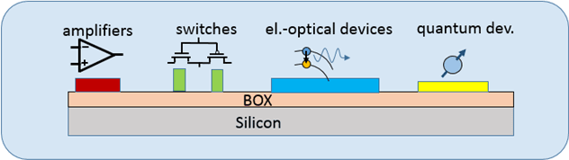
In order to combine the best of both worlds, III–V integration on Si is of great technical as well as economic interest and has been pursued for many years. A visionary example of embedded device integration is illustrated schematically in the first figure. Close proximity of III–V devices with Si-based circuits can improve system performance or even enable new application areas. It is also anticipated that system fabrication costs will be significantly lower than discrete chip packaging approaches.
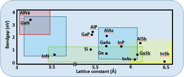
Accordingly, many different approaches towards this goal have been developed, ranging from the mechanical transfer of III–V device layers to a Si wafer as well as growing epitaxial films directly on Si. One of the key challenges to epitaxial approaches is to overcome material defects stemming from the crystal lattice mismatch with Si. The second figure shows the lattice constant and bandgap of various important III–V compounds, including Si.
Schematic illustration of the various application spaces of III–V materials and devices on Si.Bandgap versus lattice constant of several semiconductors of technological relevance. The greater the difference in lattice constant between two materials, the more challenging their co-integration.Template-assisted selective epitaxy (TASE)
We have developed an epitaxial growth method to deposit III–V materials on Si, which results in good material quality and is compatible with CMOS processes.
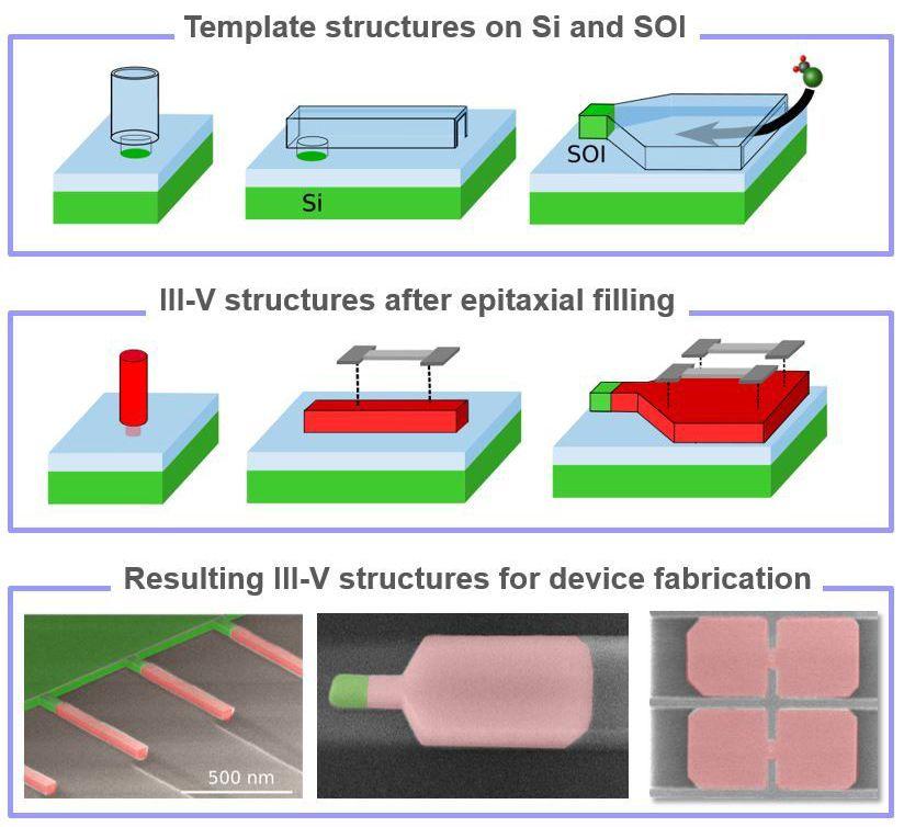
With the template-assisted selective epitaxy (TASE) method, the III–V material is deposited selectively on a small (Si) seed crystal, which can be located on a Si or silicon-on-insulator (SOI) wafer. Continuing from this nucleation step, the III–V crystal grows further and expands into the predefined template until it fills the entire cavity.
Schematic of template-assisted selective epitaxy and experimental results.
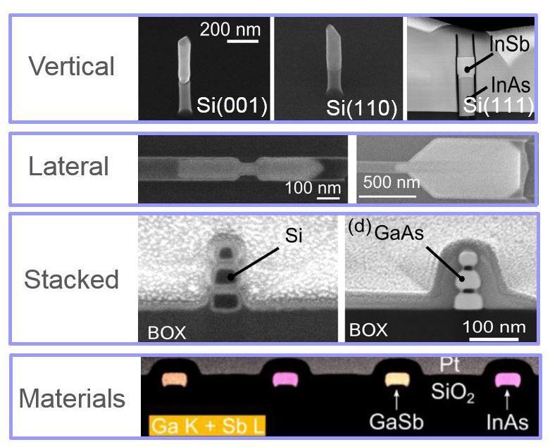
The figure below shows the design flexibility of the process, that enables vertical, planar or stacked growth of nanostructures. A sequential growth process can be used if multiple materials are desired, for example to obtain dedicated FET-channel materials targeted for high electrons or hole mobility.
Examples of III-V on Si integration using templates.Growth dynamics
A good understanding of the epitaxy process is essential for enabling high-performance materials and devices as well as for developing strategies for cointegration.
We have previously studied the growth of “bottom-up” III–V nanowires using selective area growth (SAG) in oxide mask openings. Whereas this SAG yields NWs free from detrimental structural defects, attainable NW geometries, surface and growth orientation are very limited because of surface diffusion and reaction kinetics of the precursor molecules and nanowire-free surface energies. This has inspired us to develop an alternative method based on epitaxy in templates that can alleviate many of the above constraints.
We started with the initial demonstration of III–V heterostructures on Si(111) in a SiO2 template and have progressed to much more complex structures, devices and integration schemes. We found that the crystal growth in the template follows classical crystal growth physics. After initial nucleation, favorable growth planes develop and, depending on the growth conditions, prevail throughout the filling process.
The material delivery from the gas phase mixture into the template differs from classical selective-area growth or bottom-up nanowire growth processes because of the long surface diffusion path on the template and very small exposed III–V surface.
Crystal quality
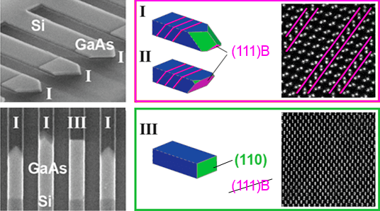
The formation of crystal defects is one of the key challenges in CMOS compatible III–V integration due to its effect on reliability and device performance. Whereas TASE avoids defects such as threading dislocations and antiphase boundaries, planar defects are commonly observed in our structures. Thus, a profound understanding of the growth dynamics is required to control the crystal stacking and prevent unintended zinc-blende-wurtzite (ZB-WZ) intermixing.
We investigated the crystal quality of TASE-grown GaAs NWs dependent on growth conditions such as temperature and V/III ratio. NWs can be categorized according to the obtained growth facets, which typically consist of a single(110) plane or a combination of (110) planes together with a (111)B plane. The former type can grow without the formation of planar defects, resulting in a pure ZB crystal. NWs exhibiting (111)B facets typically show a large number of stacking faults independent of the growth conditions.
Growth facet formation in TASE. A single (110) growth front results in defect-free material.Electronic and nanophotonic device demonstrations
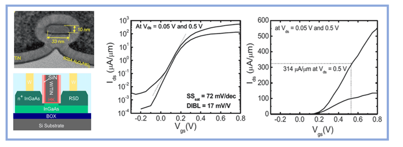
Implementing above integration concepts, we have designed and fabricated various electronic and opto-electronic devices which benefit from the use of III-V compounds. We have shown record InGaAs field effect transistors (FET) integrated on Si wafers as well as more exotic device concepts based on electron tunneling (TFET) showing superior performance over Si.
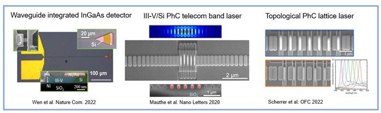
High performance InGaAs field effect transistors on Si (IEDM 2018)Embedding a III-V compound with a direct bandgap material on Si is particularly valuable for photonic applications. A few photonic examples based on our integration path are shown below. We have fabricated high-speed light detectors based on an in-place grown PIN diode, as well as novel laser structures that implement photonic crystal designs.
Electro-optical devices for integrated photonicsPublications
- Noelia Vico Triviño
- Svenja Mauthe
- et al.
- 2020
- ECOC 2020
- M. Scherrer
- Noelia Vico Triviño
- et al.
- 2021
- Applied Sciences
- Svenja Mauthe
- Preksha Tiwari
- et al.
- 2020
- Nano Letters
- Philipp Staudinger
- Svenja Mauthe
- et al.
- 2020
- Nanotechnology
- Philipp Staudinger
- Kirsten E. Moselund
- et al.
- 2019
- Nano Letters
- Philipp Staudinger
- Svenja Mauthe
- et al.
- 2018
- Nano Letters
- Svenja Mauthe
- Heinz Schmid
- et al.
- 2018
- Device Research Conference 2018