Photonic devices
In addition to the deposition and functional characterization of electro-optical materials, we have developed and realized concepts of bringing such layers into Si- photonic structures. The strong Pockels coefficient of barium titanate thin films can ultimately result in a new generation of compact, integrated devices with superior switching and optical memory properties.
Our research is focused on what are known as slot waveguide structures to achieve enhanced optical confinement in the BaTiO3 layer and to reduce the optical bending losses (Fig. 1). Based on this waveguide geometry, our work focuses on manufacturing passive and active devices such as grating couplers, Mach–Zehnder interferometers, and ring resonators [1].
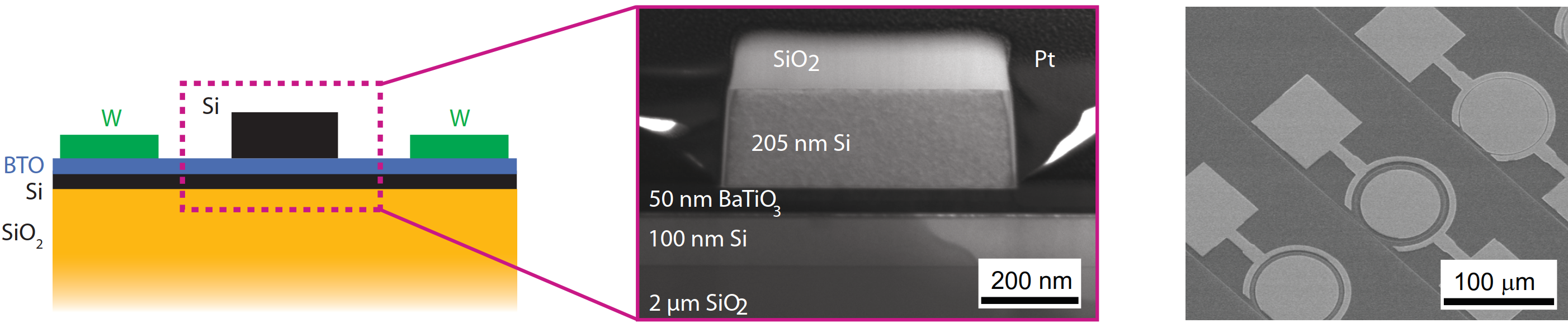
Figure 1. (Left) Schematics of a hybrid BaTiO3/Si slot waveguide structure with tungsten electrodes on the side of the waveguide. (Center) Transmission electron microscopy image of the waveguide core. (Right) Scanning electron microscopy image of several ring resonator structures. (from [1]).
A major challenge for this type of waveguide structures are the typically large propagation losses of more than 50 dB/cm (Fig. 2, left). We identified the thin strontium titanate interfacial layer commonly used to enable the epitaxial growth of BaTiO3 on silicon as a major source of absorption. By adjusting the waveguide fabrication process we developed low-loss BaTiO3/Si waveguides required for large scale integration [2].
Active switches are obtained by applying an electrical field to the active BaTiO3 layer in the waveguide region. Indeed, the waveguide mode index changes as a function of the applied voltage, as for example visible in the shifts of the resonance wavelength in BaTiO3/Si ring resonator structures (Fig. 2, right). We demonstrated that such devices can be used for high-speed modulation [3] and ultralow-power optical tuning [1], and that the Pockels effect is the main physical origin of the electro-optical switching in such devices. In addition to investigating individual devices on dedicated research wafers, we showed how to integrate BaTiO3 photonic components on photonic integrated circuits (PICs) in a CMOS-compatible fabrication route [4].
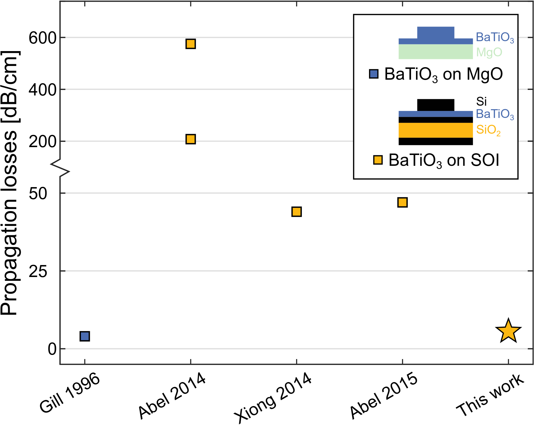
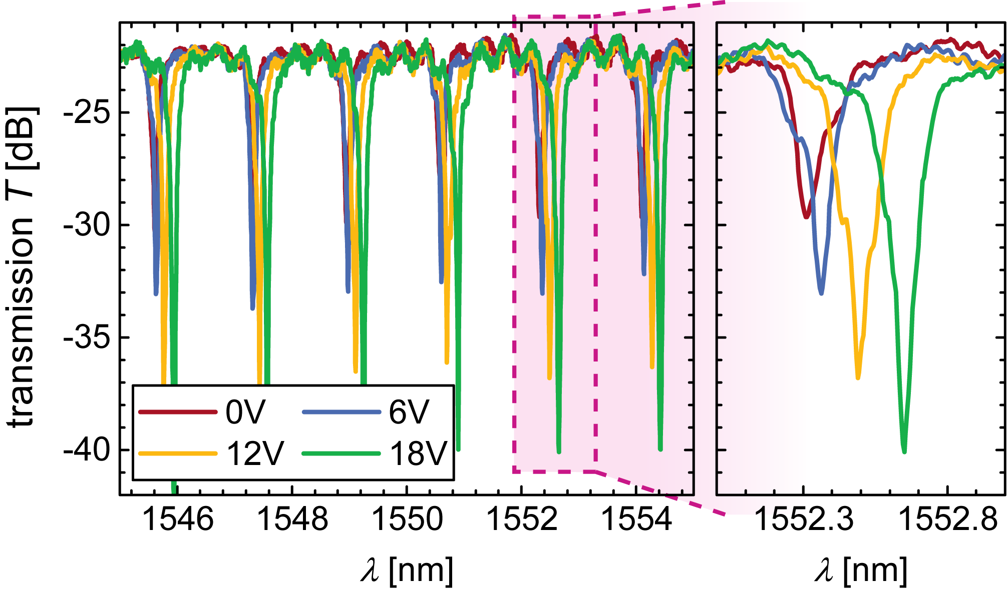
Figure 2. (Left) Comparison of previously reported propagation losses in BaTiO3-based waveguides on MgO and Si substrates. With our fabrication process we are able to achieve BaTiO3 waveguides in silicon photonic structures with low propagation losses [2]. (Right) Transmission spectra of an active racetrack resonator. Applying a voltage results in a spectral shift of the resonances, with a tunability of 18 pm/V [1].
Plasmonic switches
In addition to photonic devices, we are also working on integration of BaTiO3 in high-speed plasmonic switches. We have demonstrated very compact high-speed plasmonic modulators with low power consumption by utilizing the large Pockels effect as well the stability and durability of BaTiO3 thin films [5]. These devices feature strongly improved stability compared to alternative plasmonic switches based on other active materials such as nonlinear polymers.
[1] S. Abel et al., “A Hybrid Barium Titanate–Silicon Photonics Platform for Ultraefficient Electro-Optic Tuning,” J. Light. Technol. 34, 1688–1693 (2016).
[2] F. Eltes et al., “Low-Loss BaTiO3–Si Waveguides for Nonlinear Integrated Photonics,” ACS Photonics 3, 1698 (2016).
[3] S. Abel et al., “Large Pockels effect in micro- and nano- structured barium titanate integrated on silicon,” Nat. Mater. 18, 42–47 (2019).
[4] F. Eltes et al., “A novel 25 Gbps electro-optic Pockels modulator integrated on an advanced Si photonic platform,” in IEEE International Electron Devices Meeting (IEDM) 601–604 (2017).
[5] A. Messner, F. Eltes, F. et al., “Plasmonic Ferroelectric Modulators,” J. Light. Technol. 1 (2018).
Ask the experts

Bert Jan Offrein
Manager Neuromorphic Devices & System group
Projects & collaboration

EU FP7 project Sitoga
Silicon CMOS compatible transition metal oxide technology for boosting highly integrated photonic devices with disruptive performance

Swiss project PADOMO
Plasmonic Active Devices based on Metal Oxides

PHRESCO
PHotonic REServoir COmputing