
- Stefan Abel
- Felix Eltes
- et al.
- 2018
- Nature Materials
Electro-optic Materials on Silicon
Archived
Overview
Complex oxides show various properties that are appealing for a wide range of applications, such as high-temperature super-conductivity, interfacial two-dimensional electron gases, ferromagnetism, tunable permittivities, pyro-, ferro- and piezoelectricity, and metal-insulator transitions.
At IBM Research Europe in Zurich, we have a long history and profound experience of integrating oxide materials on silicon substrates. Such integration brings exciting material properties to CMOS-compatible fabrication processes, which ultimately enables novel electronic and optical device concepts.
In this respect, one of our missions is to advance current photonic device technology by adding materials with strong electro-optic effects to silicon photonic structures. There are two different effects that we are exploring, the Pockels effect and metal–insulator transitions.
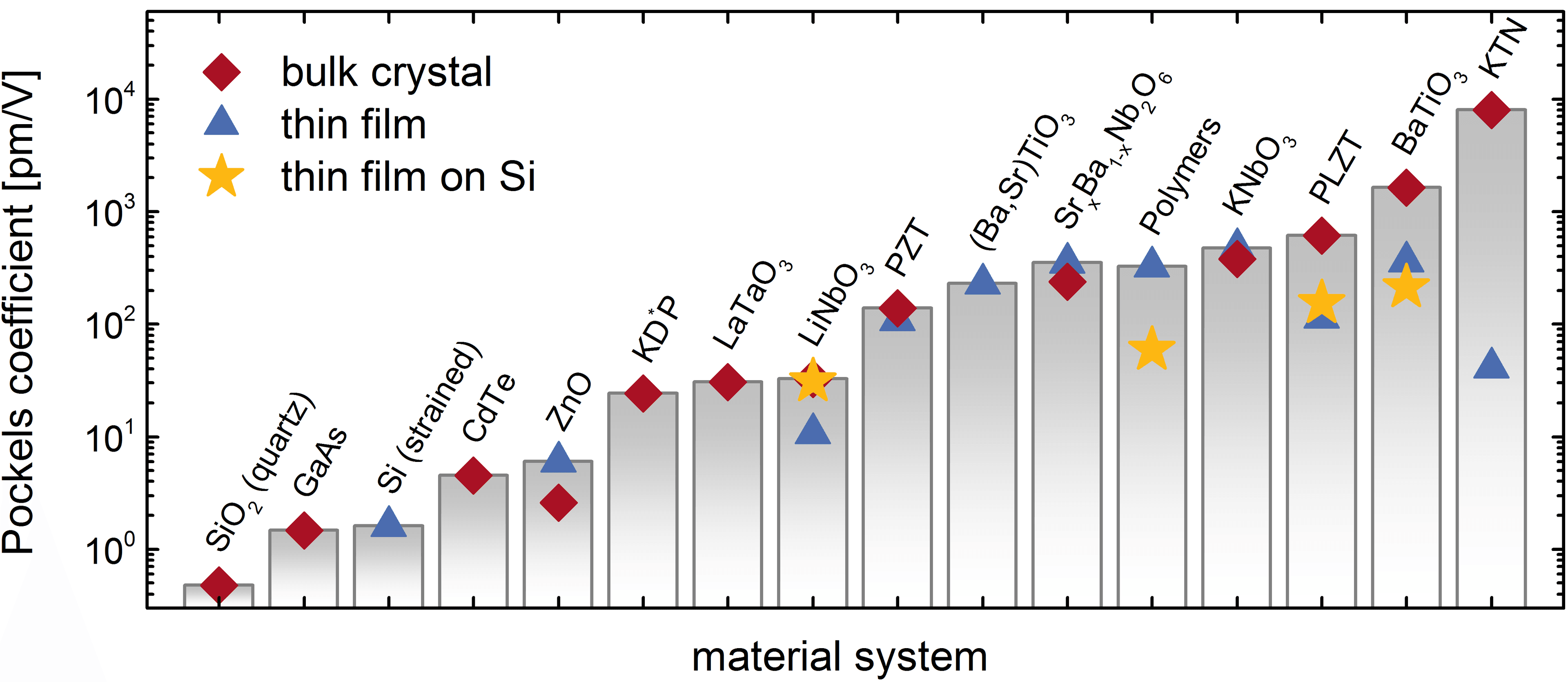
The Pockels effect allows extremely fast electo-optical modulation und efficient switching. The success of the Pockels effect can be seen with lithium niobate (LNO), which is a well-established material platform for long-haul communication links. Owing to the incompatibility of LNO with silicon integration, we focus our work on barium titanate (BTO) thin films epitaxially grown on silicon substrates. Barium titanate has one of the largest Pockels coefficients among all oxides.
Comparison of literature values for the Pockels effect in bulk crystals and thin films for various material systemsIn addition, we are also investigating vanadium dioxide (VO2) thin films on silicon photonic structures. VO2 exhibits a metal-to-insulator transition with a strong contrast in the optical properties, which might enable ultrasmall and non-volatile optical switches.
Fabrication and functional properties
Depositing complex oxides as thin films with high crystalline quality on silicon substrates is generally challenging. The main difficulty is the formation of amorphous silicon when exposing silicon to oxygen, which prohibits any further high-quality epitaxial growth.
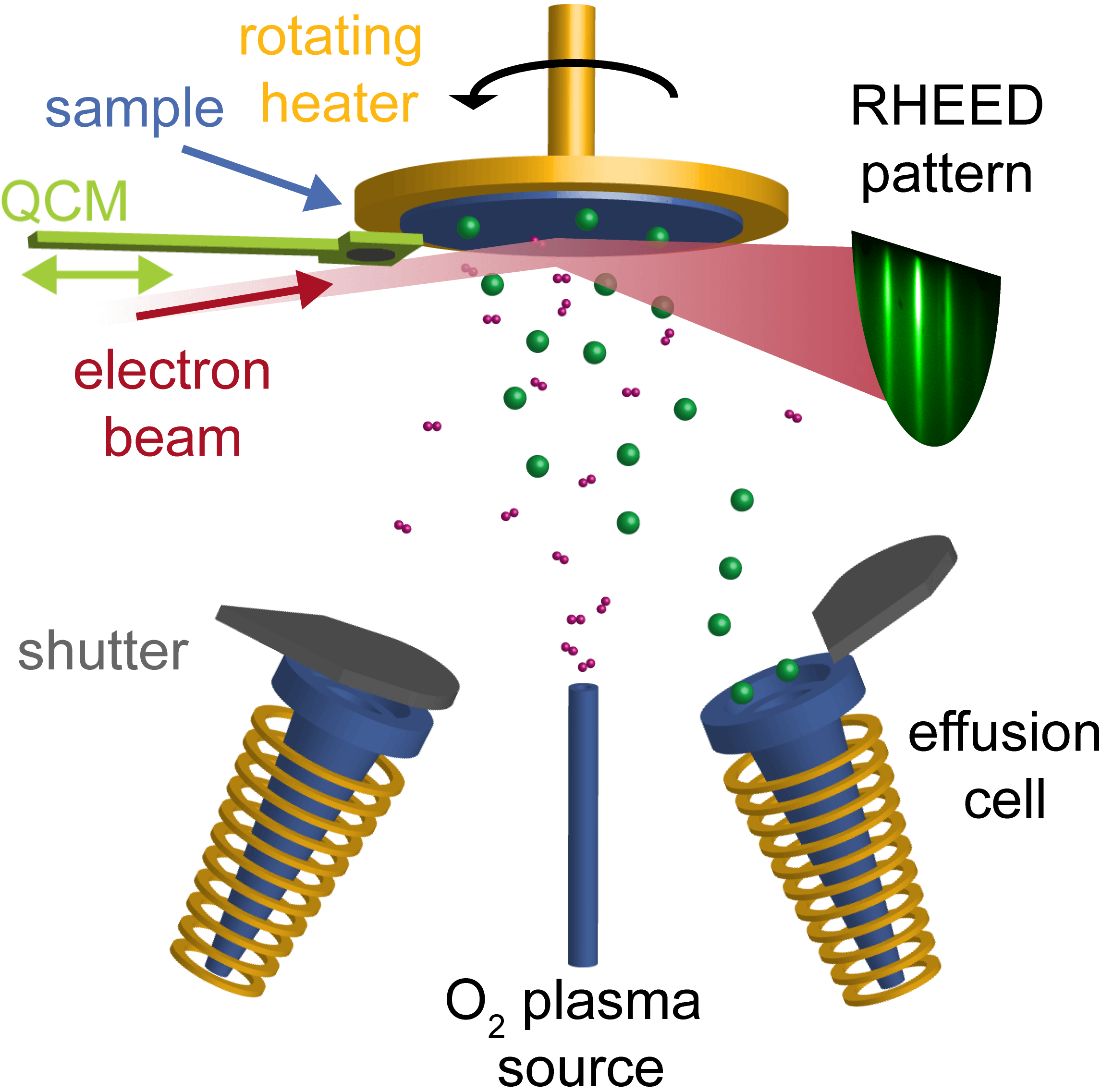
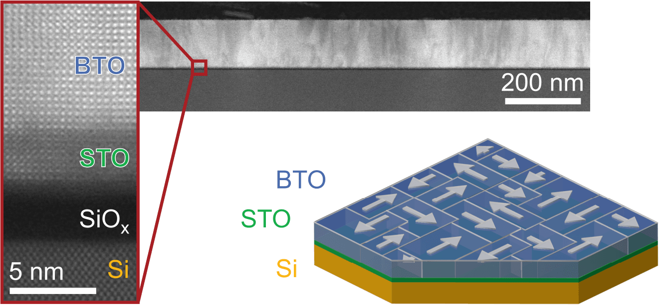
At IBM Research – Zurich, we use advanced deposition techniques such as molecular beam epitaxy (Fig. 2), pulsed laser deposition, and rf sputtering to avoid the formation of such amorphous SiOx phases. With our processes we obtain epitaxial layers of strontium titanate (SrTiO3) and barium titanate (BaTiO3) of high structural and crystalline quality directly on silicon (Fig. 2). These layers show interesting functional properties such as piezo-electricity and electro-optical activity, and serve as excellent seed layers for further deposition of other functional oxides, such as PZT.
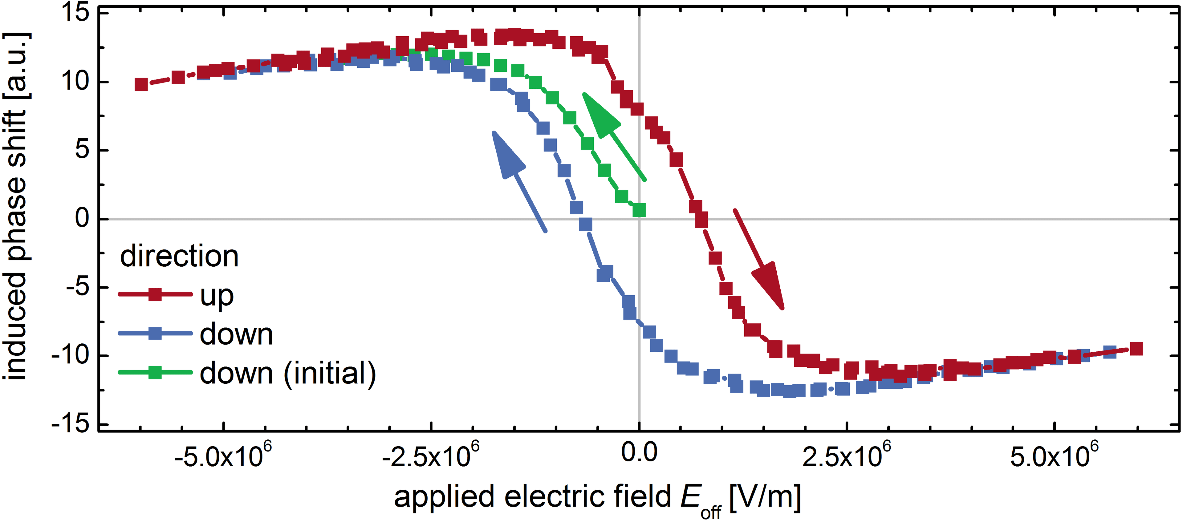
Example of a molecular beam epitaxy system.Epitaxial barium titanate on strontium titanate on silicon. The schematics shows the ferroelectric domain structure of the BaTiO3 layer.We have developed dedicated analysis techniques to determine the electro-optical and ferroelectric properties of thin films on silicon. For this we carefully measure induced changes of the birefringence of barium titanate thin films while applying an electric field to the layers. Epitaxial BaTiO3 layers typically show strong Pockels coefficients of 900 pm/V [4] and clear in-plane ferroelectricity (Fig. 3).
Our investigations also reveal a strong correlation between the functional, optical properties and the morphology and crystallinity of the films [5]. The magnitude of the Pockels effect is generally large in films of high quality.
Electro-optic response of a BaTiO3 thin film on silicon showing the ferroelectric nature of the layer.Projects & collaboration
EU FP7 project Sitoga
Silicon CMOS compatible transition metal oxide technology for boosting highly integrated photonic devices with disruptive performance
Swiss project PADOMO
Plasmonic Active Devices based on Metal Oxides
PHRESCO
PHotonic REServoir COmputing