

- Antonio La Porta
- Jonas Weiss
- et al.
- 2015
- ECTC 2015
Silicon Photonics Packaging
Archived
Overview
Various trends such as the shift to mobile applications, the Internet of Things and cloud computing imply a tremendous growth in internet data traffic. This will result in steadily increasing performance requirements on cloud data centers.
Global data-center IP traffic development from 2012 to 2017. From statista, The Statistics Portal (2014).As illustrated above, Big Data, and social media will further drive the issue of data-center performance.
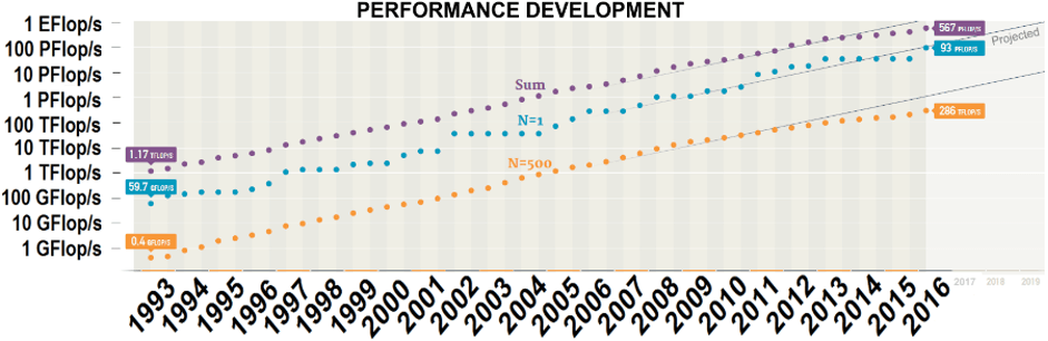
We are observing a similar trend for high-performance computers (HPC). For example, the performance of the most powerful supercomputers on the TOP500 list has increased by a factor of 10 every four years over the past 20 years.
In keeping with this trend, the first exaflop supercomputers are expected on the market by 2020. Their performance will be some 10 times higher than that of today’s fastest supercomputer, which provides 93 petaflops/s.
The “Top500” list showing performance development of the 500 most powerful supercomputers from 1993 to 2016. From the TOP500 supercomputer list of June 2016.To meet the projected performance requirements of future data centers and HPCs [3,4], the communication bandwidth needs to scale at all levels of the system, i.e., exponentially.
Consequently, there is a strong need for high-bandwidth, high-speed interconnects between racks, on backplanes, daughter cards, carriers, and ultimatelly at the chip level. Optical link technology offers fundamental advantages in scaling, bandwidth, density, and power efficiency compared with established electrical interconnects [5].
Today’s computer systems are largely based on multimode optical link technology at a VCSEL wavelength of 850 nm. To increase the “bandwidth length” product of optical interconnects in future high-performance systems, single-mode technology is becoming increasingly attractive. The emergence of silicon (Si) photonics is supporting this trend.
To meet system-cost and power constraints, a high level of integration will be required, which in our view can be achieved with the following two technologies:
- CMOS-based Si photonics using Si-On-Insulator (SOI) technology.
- Optical printed circuit board (PCB) technology using optical polymer waveguides.
Si photonics is an emerging integrated-optics technology platform based on an SOI structure, in which a wide variety of optical and electro-optical functions can be densely integrated. Optical PCB technology is an extension of established electrical PCB technology with optical signal distribution capability.
Optical PCB technology based on polymer waveguides
Earlier work: multi-mode polymer waveguides for board-level optical interconnects
In the past decade, optical printed circuit boards (PCBs) based on multimode (MM) optical polymer waveguides (PWGs) attracted increasing attention in the field of board-level optical interconnects, mainly because optical PCBs are a key enabler for electro-optical integration. In detail, they can simultaneously provide electrical and optical signal routing capability as well as enable the simultaneous interfacing of electrical and optical connections. Generally speaking, they allow a tight integration of electrical and optical functions. Moreover, one-step mating of numerous optical interfaces becomes feasible. Finally, integrated PWGs help to avoid cumbersome cable handling at board level.
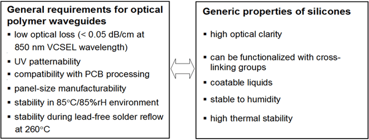
Stringent requirements for MM PWGs used as optical interconnects. This illustrates why silicones are excellent base materials to realize optical PCBs. Within a close collaboration with our polymer materials provider Dow Corning Corporation, we were able to identify suitable silicone-based optical polymers and tailor them to fulfill all requirements.The IBM photonics team has more than ten years’ experience in the research and development of such optical interconnects for board-level applications using silicone-based low-loss MM PWGs at 850-nm-VCSEL wavelength.
Within the scope of this work, we have established cost-efficient PCB-compatible manufacturing processes for panel-sized rigid or flexible optical PCBs, low-cost alignment and assembly concepts, and a standardized connector technology.
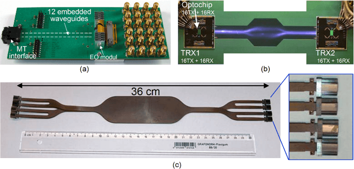
Furthermore, various passive and active optical interconnect demonstrators with high-bandwidth could be realized that use MM PWGs in or on top of mechanically rigid (Fig. 1a–b) as well as flexible (Fig. 1c) optical PCBs.
(a) Optical transmitter card of a 1210-Gbit/s optical link demonstrator containing 12 embedded PWGs. (b) High-speed and low-power link demonstrator TERABUS (funded by DARPA) with two “optochips” linked by 32 on-board high-density PWGs (with 62.5 µm pitch). (c) Optical backplane of 192 channels with complex channel shuffling based on eight stacked PWG flexes (after connectorization).Later work: single-mode PWGs for Si-photonics packaging
Recently, in order to enable the required bandwidth increase of future data centers and HPCs and to meet system-cost and power constraints, we established a novel low-cost electro-optical packaging approach for emerging CMOS-compatible Si-photonics transceiver chips.
However, one of the main challenges of Si photonics is to optically connect the Si photonics chip with the external world.
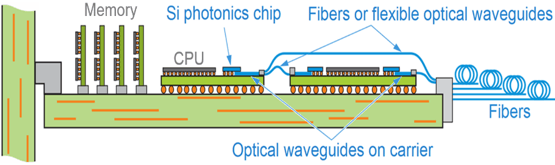
In our packaging approach where the Si photonics chip sits next to the CPU on a joint carrier, we direct the light by adiabatic optical coupling from the Si waveguides to dedicated SM PWGs and from there to SM fibers at the carrier or board edge, as schematically shown below.
Novel electro-optical Si photonics packaging approach for high-bandwidth (up to 10 Tbit/s) off-carrier optical communication. Optical SM PWGs are used to connect a Si photonics transceiver chip with the external world.This method allows us to overcome the problem of dimensional and modal mismatch between the SM fibers and the much smaller Si waveguides.
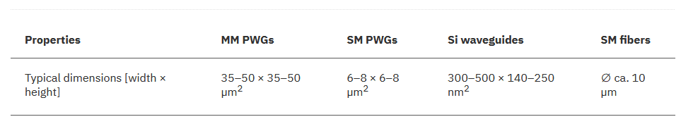
Comparison of dimensions between multi-mode and single-mode polymer waveguides.To realize the required SM PWGs, we extended our well-established 850-nm VCSEL-based MM PWG technology to SM PWGs operating around 1310 nm as well as 1550 nm wavelength (i.e. in the O and C bands).
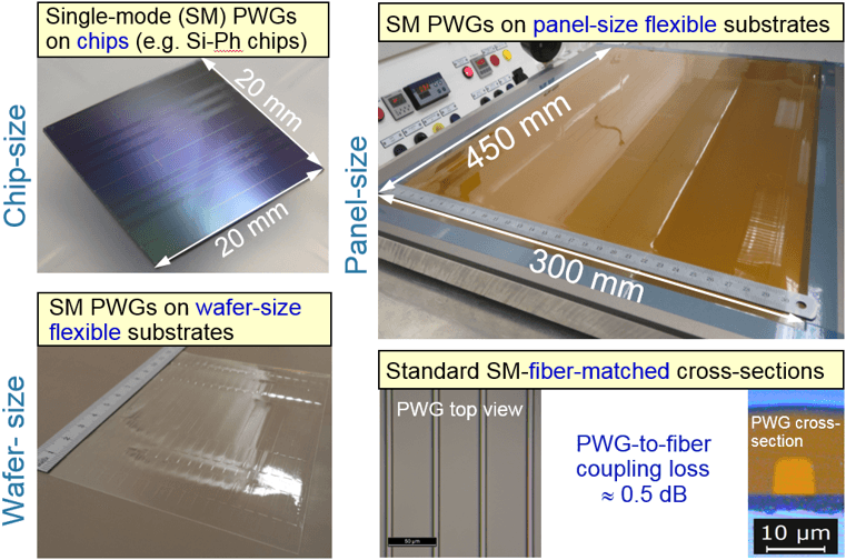
Processing of the SM PWGs (Fig. 3) is fully compatible with PCB technology. PWGs are reliable in harsh 85°C/85%rH tests (telcordia standard) as well as in temperature cycles of lead-free soldering (up to 260°C). Our SM PWG technology supports processing on chip-level, wafer-level and even on full panels (e.g. 450 × 300 mm2), as depicted in Fig. 4.
Depending on the application and the substrate choice, rigid as well as flexible PWG boards/chips can be implemented.
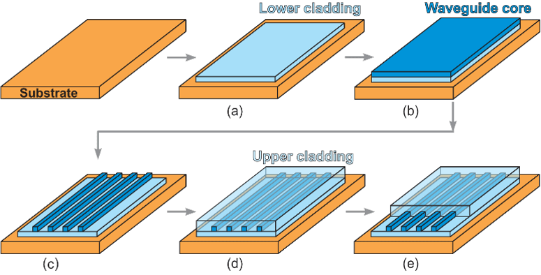
Schematic of SM PWG manufacturing process. (a) Deposition of lower cladding polymer followed by UV-flood curing. (b) Deposition of waveguide core polymer. (c) Waveguide patterning by UV-laser direct writing or proximity-mask lithography, followed by solvent-based development. (d) Deposition of upper cladding polymer. (e) UV-flood curing, or optionally UV patterning and solvent-based development of upper cladding. Finally, thermal curing step.Photographs of SM PWGs realized on chip, wafer, and panel levels.Adiabatic optical coupling
Integrated CMOS-based silicon (Si) photonics monolithically combines electrical and optical functions on a single Si chip. Silicon photonics is regarded as the top candidate to provide bandwidth scalability by the fundamental scale-out properties of integrated technology and by introducing additional functions such as wavelength division multiplexing (WDM) or higher-order modulation formats. All necessary Si-photonics building blocks have been already demonstrated.
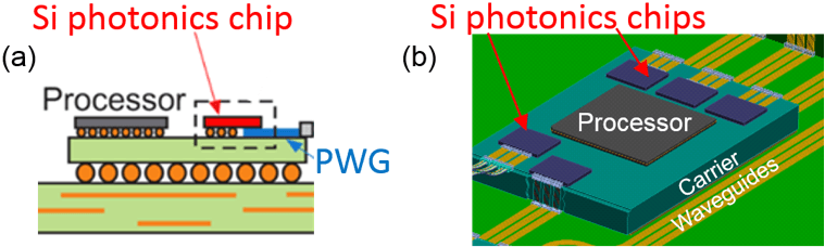
To enable cost-effective and scalable system-level integration of Si-photonics transceiver chip, we establish a radically new approach in which a Si-photonics chip is co-packaged with the data-processor chip directly on a carrier substrate.
System-level integration schemes of Si-photonics chip co-packaged on a processor package.Such tight electro-optical integration can provide off-carrier bandwidth in excess of 10 Tb/s. This is obtained by increasing the number of physical optical channels and exploiting the WDM capabilities offered by Si photonics.
The Si-photonics chip is now co-packaged with the ASIC CPU or switch chip. This allows a smaller footprint and hence results in a higher bandwidth density. Improved electrical signaling is also obtained because of the short electrical interconnects with fewer interfaces between the electro-optical transceiver and the data processing elements.
As our objective is to realize scalable system-level integration, as depicted in the figure above (left side), a new optical interface approach needs to be provided. We target an optical coupling scheme that can enable broadband and efficient coupling between a large number of on-chip Si waveguides and the external world.
Single-mode (SM) polymer waveguides (PWGs) are used to distribute the optical signals between the various subsystems across the optical printed circuit board (PCB) and to establish the interface between the Si-photonics chip and the fiber cables.
The figure above shows a scheme of the envisioned system-level package approach (right side).
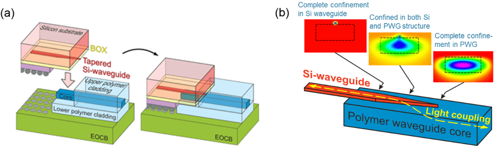
The large optical modal mismatch between the on-chip Si waveguide (typically measuring a few hundred nanometers in height and width) and a larger SM PWG mode-matched with a standard SM fiber (approx. 10 µm), can be solved by realizing an adiabatic transformation of the optical mode of a Si-waveguide to the mode of the SM PWG. This is accomplished by inverse tapering the Si-waveguide end and bringing it in very close proximity or in direct physical contact with the PWG.
The second figure shows a scheme where a Si-photonics chip is attached to a carrier with PWGs. The optical power of the guided mode in the Si waveguide is transferred to the mode of the SM PWG because the Si-waveguide width is slowly tapered to reduce its effective index.
This method is fully compatible with established electrical assembly techniques (e.g., solder-reflow, flip-chip bonding). It allows simultaneous electro-optical interfacing and is scalable to many optical channels.
(a) Schematic of the Si-photonics chip assembly to the carrier with SM PWG processed. (b) Close-up of the Si-to-PWG core configuration scheme for the adiabatic optical power transfer.Recent works were published targeting specifically a Si-waveguide-to-PWG system with multiple optical I/Os. We reported on the design, fabrication, and experimental proof of concept of adiabatic optical coupling between an array of Si-waveguides in a Si-photonics chip and an array of SM PWGs.
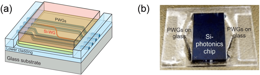
The Si-photonics chip was flip-chip bonded onto SM PWGs processed on a separate substrate, as shown in the figure below.
(a) Flip-chip bonded Si-photonics chip on a separate chip containing PWG scheme and (b) sample.Optical coupling losses ≤1 dB for adiabatic optical couplers with taper lengths ≥1.0 mm were measured. Low-loss optical coupling was verified experimentally in the spectral window of the O-band (around 1310 nm) and C-band (around 1550 nm) for both TE and TM polarized light.
Furthermore, this optical coupling scheme is tolerant against lateral misalignment of the Si chip with respect to the polymer waveguide structures. A misalignment of ±2 μm led to a loss increase of only less than 1 dB. Negligible optical back reflections (<50 dB) were found from the adiabatic coupler.
Projects & collaboration
ROAM
Revolutionising optical fibre transmission and networking using the Orbital Angular Momentum of light
WIPE
Wafer scale Integration of Photonics and Electronics
CarrICool
Modular interposer architecture providing scalable heat removal, power delivery and communication
ITC Streams
Silicon Photonics Transceiver and Routing technologies for High-End Multi-Socket Server Blades with Tb/s Throughput interconnect interfaces
Publications
- Antonio La Porta
- Roger Dangel
- et al.
- 2016
- OFC 2016
- Antonio La Porta
- Roger Dangel
- et al.
- 2016
- ECTC 2016
- Roger Dangel
- Jens Hofrichter
- et al.
- 2015
- Optics Express
- Roger Dangel
- Antonio La Porta
- et al.
- 2018
- IEEE JSTQE
- Konstantinos Papatryfonos
- David R. Selviah
- et al.
- 2021
- Applied Sciences
- Christos A. Thraskias
- Eythimios N. Lallas
- et al.
- 2018
- IEEE Commun. Surv. Tutor.