SiTe
Overview
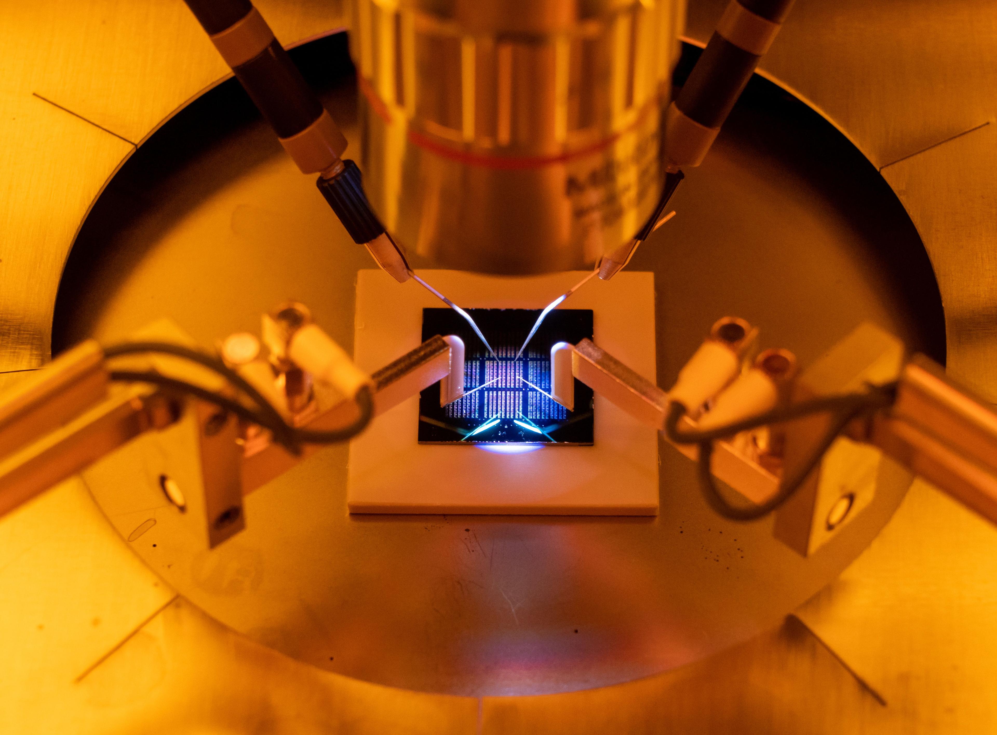
The SiTe project, led by the principal investigator Matthias Mergenthaler, is focusing on developing scalable silicon-based semiconductor-superconductor hybrid weak links with the aim to realize novel and more scalable qubit technology incorporating them. This project has received funding from the European Union’s Horizon 2020 research and innovation programme under the Marie Sklodowska-Curie grant agreement No 899018. It is hosted at IBM Research GmbH in Rüschlikon (Switzerland) and leverages its unique infrastructure for device fabrication (Binning and Rohrer Nanotechnology Center) and low temperature device characterization.
The project has three main objectives:
- The development of semiconductor-superconductor hybrid weak links based purely on silicon.
- The characterization of these silicon based weak links via DC bias and microwave spectroscopy.
- The implementation of such elements into larger quantum devices to realize novel qubits.
One of the first milestones was to realize a contact to an intrinsic silicon channel that exhibits superconductivity. For this material characterization of superconductors and metal-silicides was carried out. Some of these silicides already exhibit superconductivity by themselves and form a clean interface to the silicon channel, providing a contact for either p- or n-type charge carriers. Additionally, bi-layers of metal-silicides and large gap superconductors were investigated to assess their material properties.
Superconductivity of metal-silicides. (left) Optical image of PtSi Hall bar. (right) Critical temperature measurement of PtSi.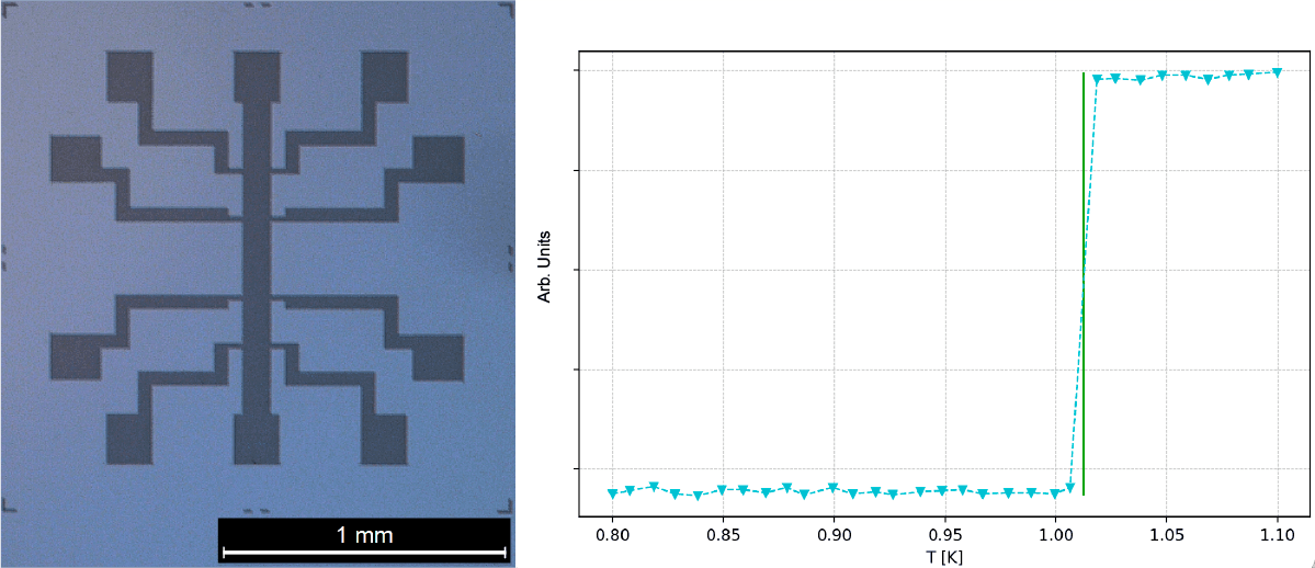
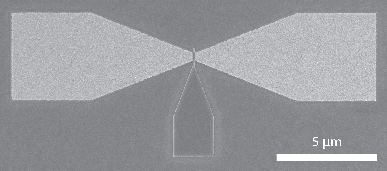
Integrating such contacts exhibiting superconductivity with silicon transistors fabricated with CMOS standard processes in order to realize a superconducting weak link through silicon was a second milestone achieved within this project. First characterizations of such a device show clear signs of superconducting transport properties through the silicon channel.
Silicon finFET transistor made with PtSi contacts.