Topological qubits
Hybrid semiconductor-superconductor materials are a promising platform for quantum computing applications. Planar Josephson junctions in these materials can coherently and ballistically transport a supercurrent, which is controllable with a gate voltage. This allows for a gate-tunable superconducting qubit. Discrete microscopic states are also present within the junctions, which can be addressed directly to create an Andreev qubit. Further, in the presence of magnetic fields these materials can host topological states. This paves the way to a topologically protected qubit, where the coherence time is independent of local noise fluctuations.
Material and device fabrication
Two-dimensional heterostructures allow for great flexibility with device design and scalability, compared with nanowires. We use an MBE-grown InAs 2D-electron-gas, which has epitaxially matched Al deposited in situ for a high-quality interface between the superconductor and semiconductor materials. We lithographically pattern devices by selectively etching the top Al layer to expose the 2DEG below. The electron density in these regions can then be controlled via metallic gate electrodes, which are deposited on top of an insulating dielectric layer.
Multi-messenger sensing of ABSs
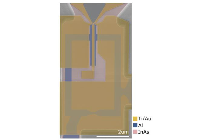
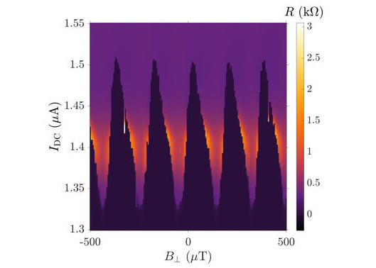
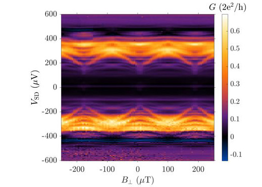
Discrete Andreev bound states carry the supercurrent across the Josephson junction. The properties of these states can therefore be inferred from the characteristics of the supercurrent under the influence of external parameters. For example, highly transmissive ABSs give rise to a current phase relation (CPR) which is non-sinusoidal. We can measure this by measuring the supercurrent as a function of the field threading a superconducting loop containing the junction, as in the SEM image.
Tunnelling spectroscopy of Andreev Bound States
In addition to inferring the ABS properties, we can measure them directly via tunnelling spectroscopy. As a function of flux, ABSs evolve within the superconducting gap. With proper control, using a gate voltage and a magnetic field, the rich physics of these ABSs can be harnessed to build devices for quantum computing applications.
Investigating PbTe nanowires
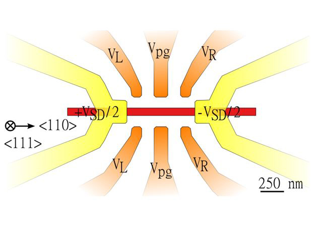
Topological quantum computing is based on a class of quasiparticles: Majorana bound states. Due to its bulk material properties, lead telluride (PbTe) is a promising candidate for the investigation of Majorana bound states. There are six gates (orange), which are used to tune the electrostatic potential of the nanowire (red) locally. Furthermore, there are contacts on both ends of the nanowire device (yellow). With the leftmost and rightmost gates VL and VR, small regions of the nanowire are depleted, enabling the formation of a quantum dot between these depleted regions. The central plunger gates VPG tune the filling of the energy levels of the quantum dot.
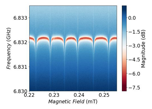
Microwave sensing of Andreev bound states
Microwave spectroscopy measurements of Andreev bound states complement low frequency methods as tunneling spectroscopy. To perform the microwave spectroscopy measurements of Andreev bound states, a superconducting microwave resonator is coupled to a Josephson junction embedded in a superconducting loop. Since qubit implementation requires microwave signals, the characterization of the system with such frequencies is a further step towards the realization of a quantum processor.
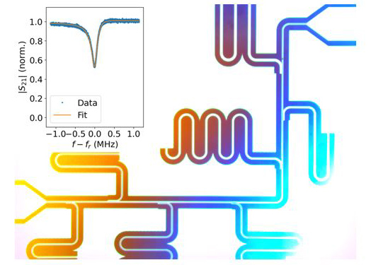
Superconducting microwave resonators for high frequency measurements
Read-out of superconductor semiconductor hybrid qubits, e.g. Andreev qubits, can be realized by coupling the qubit to a microwave resonator. For the purpose of scaling superconducting microwave resonators, they can be multiplexed by coupling several of them to a common transmission line. The fabrication of the high-quality resonators is done in our Binnig and Rohrer Nanotechnology Center.
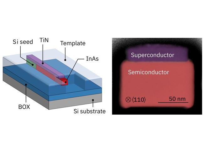
Monolithic integration of III-V semiconductor nanostructures on a Si/SiO2 platform with superconducting elements
Based on the template-assisted selective epitaxy (TASE) method, invented at IBM Research in Zurich, we developed a platform for CMOS compatible fabrication of semiconductor-superconductor hybrid devices (hybrid-TASE). In comparison to common methods, our approach is based on commercial SOI wafers and is highly scalable. The semiconducting elements of our devices are self-aligned and no further processing is required after the epitaxial growth of the III-V nanowires.
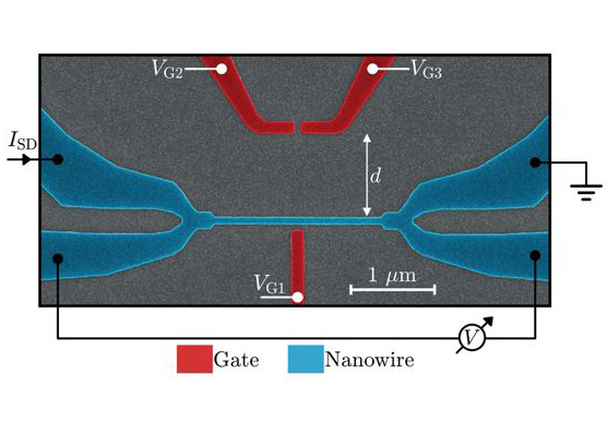
Phonon-actuated superconducting switch
We experimentally investigate fundamental properties of superconductors. A superconducting nanowire (blue) can be switched into the resistive state by applying a gate voltage VG1 or voltages +VG2 and –VG3 to the gates (red). In both cases, a small gate current on the order of 1 nA flows through the substrate and high energy electrons flow through the substrate, emitting out-of-equilibrium phonons. When high-energy electrons and phonons reach the superconducting nanowire, the channel switches from the superconducting into the normal state.
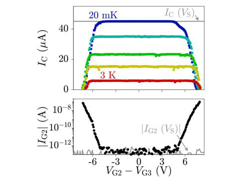
Characterizing a superconducting switch
Critical current of a superconducting TiN nanowire as a function of differential gate voltage VG2-VG3 and temperature (top). The suppression of superconductivity with increasing gate voltage is correlated to the flow of a small gate current (bottom).