Our work on alternative quantum platforms aims at technologies that have the potential to boost and complement the capabilities of superconducting qubit technology. We are also exploring new paradigms for certain types of quantum applications and linking quantum systems. Silicon quantum dots with exceptionally long coherence times that could provide very small, long-lived qubits are coming within our grasp. Electromechanical coupling combined with optomechanical coupling could be used for efficient and coherent interconversion of single microwave and optical qubits. Quantum fluids of light could serve as room-temperature quantum simulators, helping us to explore certain otherwise hardly accessible physical systems.
Semiconductor spin qubits
Coupling spin qubits to microwave photons, controlling spins with an electric field.
Quantum fluids
Realizing a scalable, easy-to-handle device platform based on polariton quantum fluids.
Quantum links
Using nano- and micromechanical oscillators to enable navigation, timing, motional sensing and wireless communication.
Topological qubits
Enhancing qubit performance by spreading a quantum state over multiple qubits at the same time.
Semiconductor spin qubits
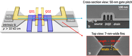
Spin qubits are one of the prospective types of qubit for future scalable quantum computers. However, reliable fabrication of these basic quantum elements is challenging and requires nearly perfect materials and nanometer precision owing to their small size and sensitivity to the electromagnetic environment. Silicon, which has been the material of choice for classical computing for many years, also has highly desirable properties for the fabrication of spin qubits.
Individually confined electron and hole spins in silicon-based quantum dots have been shown to have exceptionally long lifetimes, up to seconds or longer for electrons in isotopically purified 28Si. Thanks to the tremendous advancement of silicon technology in recent years, reliable fabrication of silicon quantum dots has come within reach. Some of the silicon transistor devices in the latest technology nodes can actually be used directly as spin qubits.
“Our goal is to engineer the quantum coupling between silicon qubits and microwave photon states.” —IBM scientist Andreas Fuhrer
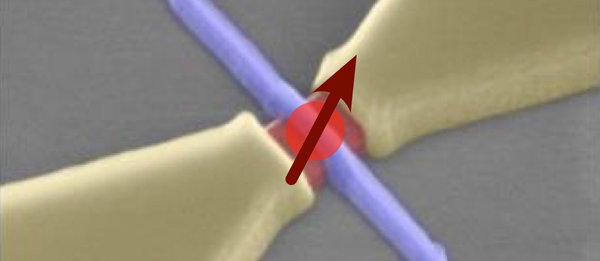
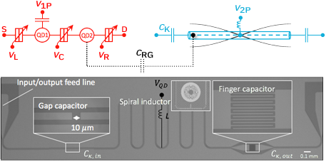
However, one of the problems that currently plagues all spin-qubit architectures is the unresolved question of long-range coupling. Such coupling is needed for the operation of a 2D qubit-lattice as required by topological surface codes that provide quantum error correction. We are investigating silicon quantum dots and their coupling to superconducting microwave resonators.
We are addressing the coupling issue and finding a link to IBM’s more advanced superconducting qubit platform development. We are also investigating the coupling of spins to surface-acoustic waves as an alternative to microwave resonators.
Controlling semiconductor spins
The spin of an electron can be used to store and process quantum information. For this, a long spin lifetime and the ability to manipulate the spins quickly and controllably are needed. These two requirements are difficult to meet simultaneously. For example, we can control spins with an electric field by using spin-orbit interaction. However, this makes spins susceptible to charge noise.
We investigate spin coherence in semiconductor quantum structures and ways to manipulate the spins without compromising their lifetime. Such manipulation can be achieved in different ways, for example through spin-orbit interaction, magnetic field gradients or hyperfine interaction to nuclear spins.
Spin-orbit interaction in semiconductors
If electrons are moved in a semiconductor material where a spin-orbit interaction is present, the polarization direction of the electron’s spin rotates. Using optical pump-probe techniques, we can measure such spin rotations in semiconductor quantum structures. The size and symmetry of the spin-orbit interaction can be determined for a wide range of semiconductor materials. Of special interest are narrow-gap materials such as InAs, GaSb and InSb that have a strong spin-orbit interaction, which is important for coupling spin qubits to microwave photons, but also for creating topologically protected states such as Majorana zero modes.
Spin helix modes in 2D and 1D
Spin-orbit interaction combined with momentum scattering typically leads to a rapid dephasing of the electron spin. By engineering the quantum confinement of the electrons, a situation can be achieved where the spins collectively precess about a single axis and form a helical spin patterned, called a persistent spin helix. As the name suggests, spin dephasing is strongly suppressed. Using spatially resolved pump-probe measurements, we have imaged the formation of a persistent spin helix that develops from a local spin excitation.
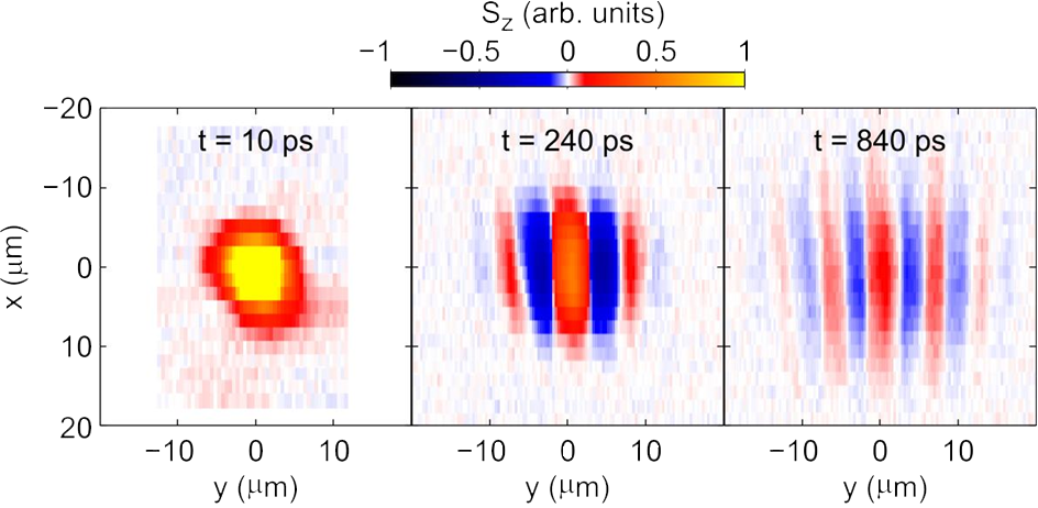
Measured time-resolved maps of spin polarization forming a persistent spin helix.
From M.P. Walser, C. Reichl, W. Wegscheider, and G. Salis, “Direct mapping of the formation of a persistent spin helix,” Nature Phys. 8, 757 (2012).
Controlling nuclear noise in semiconductor spin qubits
A semiconductor quantum dot typically consists of more than 100,000 atoms. The nuclei of these atoms have a spin that interacts with the electron spin via the hyperfine interaction. This slightly changes the energy of the spin-up and spin-down states of the electron, depending on the size and direction of the nuclear spin polarization. Because the nuclear spins randomly change their direction over time, the electron spin dephases.
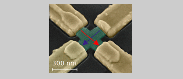
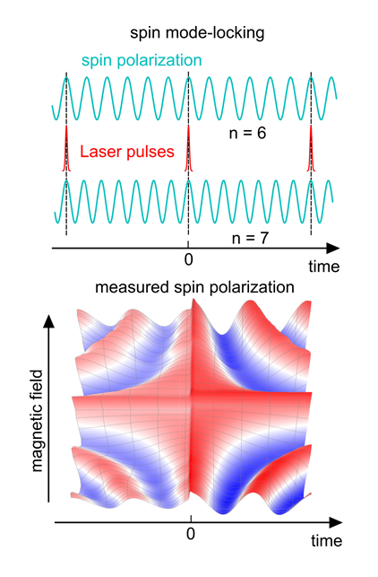
Different techniques have been developed to get such nuclear fluctuations under control and focus the nuclear spin polarization on a well-defined value. A very intriguing possibility consists of illuminating the semiconductor island with periodic laser pulses. It has been found that such illumination brings the qubit energy to a well-defined value that is directly related to the laser repetition rate. Such a locking of the qubit energy has been observed in quantum dots that contain a single electron, but the exact reason why the energy locks to the laser repetition rate has remained unclear. We have investigated this effect and have found that it is surprisingly much more universal than previously thought: We were able to observe nuclear focusing also in islands that contain many electron spins and that are fabricated using standard techniques of the semiconductor industry. This allows us to fabricate dots of well-controlled shape, size and position, which is essential in order to apply the technique to spin qubits in a scalable way.
Principle and measurement of spin mode-locking in lithographically defined quantum dots, see image.
S. Markmann, C. Reichl, W. Wegscheider and G. Salis,
“Universal nuclear focusing of confined electron spins,”
Nature Communications 10, 1097 (2019).
Ask the experts


Andreas Kuhlmann
Post-doctoral researcher
Collaboration

Quantum fluids
Quantum phenomena are at the heart of the upcoming technological wave that is going to power a new generation of smart materials and devices. Computers with “classical” hardware are not suitable and overburdened with the simulation of large quantum mechanical systems because the size of the Hilbert space is growing exponentially.
Richard Feynman was among the first to envision that quantum simulators could fill this gap, where another well-controlled and measurable system can be used to efficiently mimic and explore the physics of the otherwise inaccessible and intractable systems.
In particular, phenomena like strongly correlated and topological phases that are key to both fundamental and exotic material features such as superconductivity and the spin Hall effect are notoriously difficult to tackle experimentally and theoretically.
Although very elaborate experiments with ultracold atoms at nano-Kelvin temperatures have provided a glimpse of the potential of a quantum simulator, an approach which is much less complex and suitable to become an integrable, widely-usable technology is still missing. Compelling candidates are Bose–Einstein condensates (BEC) of exciton polaritons, which are macroscopically coherent matter waves of quasi-particles built from electron-hole pairs (excitons) and photons.
“We aim to realize a scalable, easy-to-handle device platform based on polariton quantum fluids able to simulate such systems.” —IBM scientist Thilo Stöferle
We are building on our recent demonstration of non-equilibrium BEC of exciton polaritons with an amorphous polymer at room temperature to create photonic potential landscapes for polariton condensates by harnessing novel nanostructured, tunable cavity arrays . Furthermore, the same platform allows us to use colloidal semiconductor nanoplatelets and perovskite nanocrystals to reach into the regime of strong interactions.
These new classes of materials implement the ideal compromise between high overall oscillator strength and strong exciton confinement, while at the same time offering advanced assembly options that allow us to form regular arrays. Such experiments could enable access to strongly correlated phenomena such as a quantum phase transition to a Mott insulator, which has been elusive to polariton systems up to now.
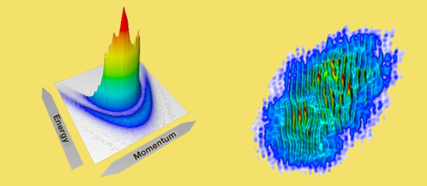
Polariton condensate
The polariton condensate appears as a nonlinearly growing peak in the momentum distribution, corresponding to the macroscopic population of the state. Interference fringes in a Michelson interferometer are a signature of the long-range spatial coherence. Pinned vortices result in fork-like dislocations.
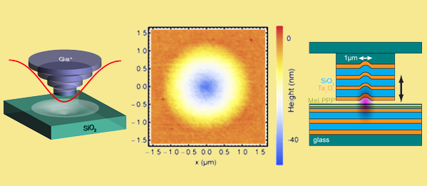
Wavelength-scale Gaussian-shaped deformation
The pattern on the left is achieved by focused ion beam milling into the substrate. Atomic force microscopy (center) reveals the smooth Gaussian structure on the top mirror substrate. By mounting both halves of the optical microcavity on xyz-nanopositioners, we create tunable polaritons in the external potential given by the nanostructure.
Ask the experts


Projects

Quantum links
In our modern information age, nano- and micromechanical oscillators are indispensable technologies that enable navigation, timing, motional sensing and wireless communication. They are used in particular for radio frequency filtering as well as for measuring rotation and acceleration and are employed commercially in cell phones, automobiles and airplanes. The quality factor of mechanical oscillators can be extremely high, even in the gigahertz range, and in general, they have unique advantages over their electronic counterparts.
In recent years, a technological and scientific revolution has occurred with respect to the efficient, coherent operation of such mechanical devices. Analogous to the previous quantum control of atoms, ions, and molecules and, later, electrical circuits, nano- and micromechanical devices can now be interrogated and controlled at the quantum level using optical fields, thus establishing the field of cavity optomechanics. By employing optical resonators that greatly enhance otherwise weak radiation pressure, the resonant build-up of laser light in an optical cavity gives rise to parametric coupling of the optical and mechanical degrees of freedom, enabling cooling, amplification, and unprecedentedly sensitive detection of mechanical motion. The latter includes microwave circuits with vibrating capacitive elements.
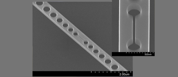
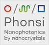
Scanning electron microscope image of a freestanding quasi-one-dimensional silicon photonic crystal nanobeam cavity with a 40-nm slot.
Cavity optomechanics
Our current research is focused on exploiting electromechanical coupling in combination with optomechanical coupling for the efficient transduction of signals from the electrical to the optical domain and ultimately extending the technology into the realm of interconversion of single microwave and optical qubits.
We are investigating photonic crystal cavities based on non-centrosymmetric materials and exploit the inverse piezo effect to actuate the mechanical modes at microwave frequencies. III–V materials are of particular interest because of the high index of refraction, transparency in the visible (for some materials), and the possibility of integration on oxide-on-silicon substrates for fabrication of photonic circuits.
Ask the expert
EU projects


Topological qubits
Information stored in the bits of a classical computer can be preserved for a very long time. In a quantum computer, on the other hand, information stored in quantum bits (qubits) is lost as time goes by. Decoherence, the tendency to lose information, is an incredibly widespread phenomenon, originating from a vast range of causes. A qubit might decohere because of internal imperfections or due to weak interactions with its surroundings. As a result, a major effort of modern quantum science aims at prolonging the qubit coherence time: The longer quantum information can be stored in a qubit, the more operations can be performed on that qubit before the information is lost, allowing increasingly challenging tasks to be addressed.
A viable strategy to enhance qubit performance consists of spreading a quantum state over multiple qubits at the same time. In this way, disturbances affecting each qubit individually will have less of an impact on the quantum state as a whole. Another promising approach that is currently under intense investigation is to realize qubits where natural protection mechanisms against decoherence are already in place. Topological insulators and topological superconductors are a novel class of materials where electronic states arise with inherent protections. These are ideal candidates for the next generation of quantum devices and quantum computers.
At IBM, we are investigating such topologically protected states, which we achieve by combining one-dimensional semiconductor nanowires and superconductors. Recent results have demonstrated the capability to grow pristine InAs nanowires integrated on a silicon substrate.
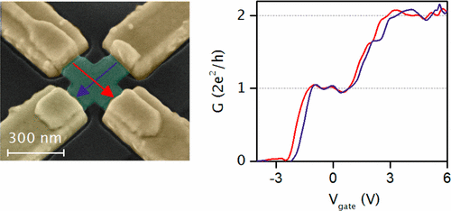
Ballistic 1D quantum transport is maintained across several junctions in
series and 1D modes can be distributed into multiple nanowire branches.
From J. Gooth et al., Nano Letters, 17(4) 2596-2602 (2017).
