AC

IBM Fellow, Vice President Europe and Africa and Director IBM Research Zurich
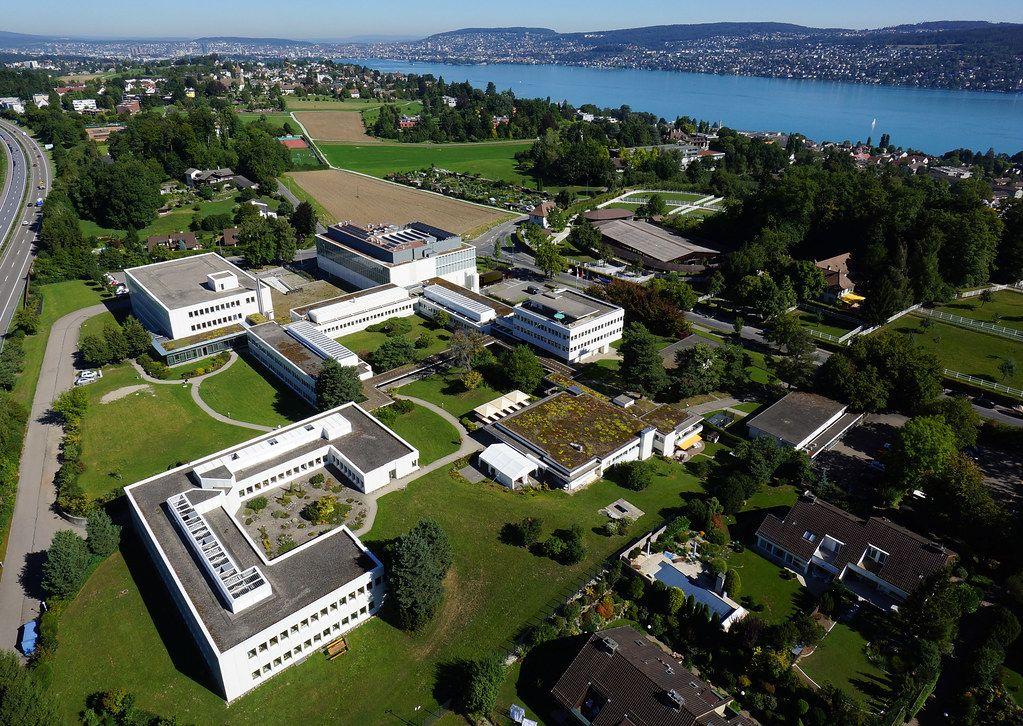
The location in Zurich is one of IBM’s 12 global research labs. IBM has maintained a research laboratory in Switzerland since 1956. As the first European branch of IBM Research, the mission of the Zurich Lab, in addition to pursuing cutting-edge research for tomorrow’s information technology, is to cultivate close relationships with academic and industrial partners, be one of the premier places to work for world-class researchers, to promote women in IT and science, and to help drive Europe’s innovation agenda.
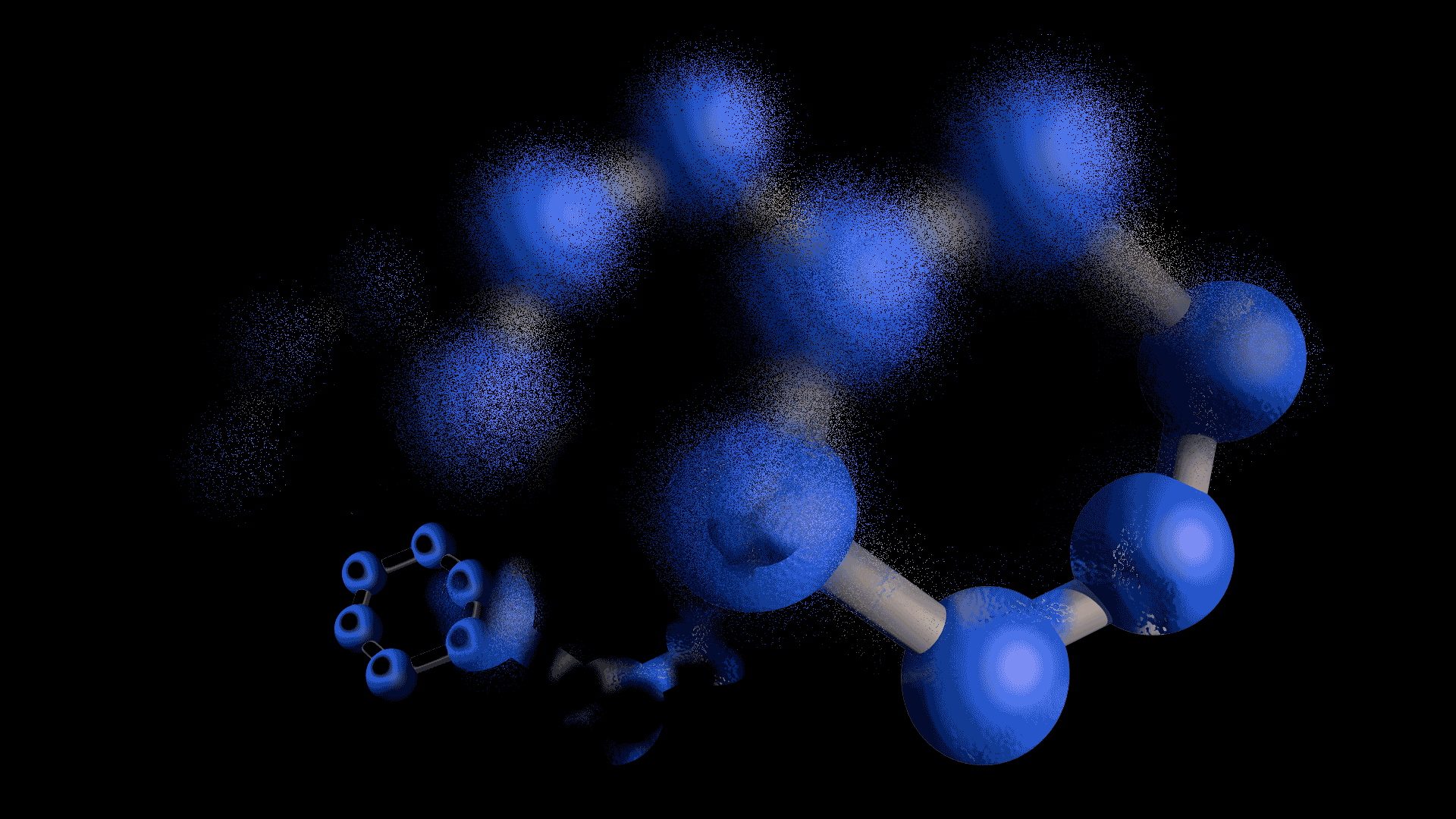
We are developing next generation Data and AI technologies for solving tough business and societal problems such as accelerating the discovery of new materials, understanding climate impact, scaling AI in business workflows, and cost/performance optimization of data intensive applications.
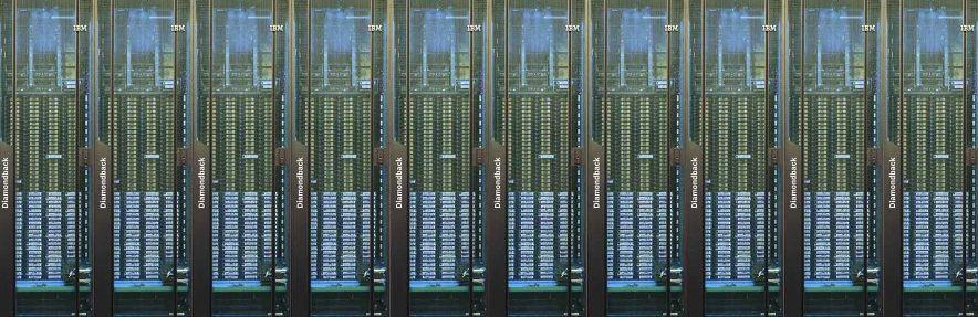
In the Hybrid Cloud Research department we drive innovation in the infrastructure for hybrid cloud, focusing on cutting-edge AI as well as storage technologies.
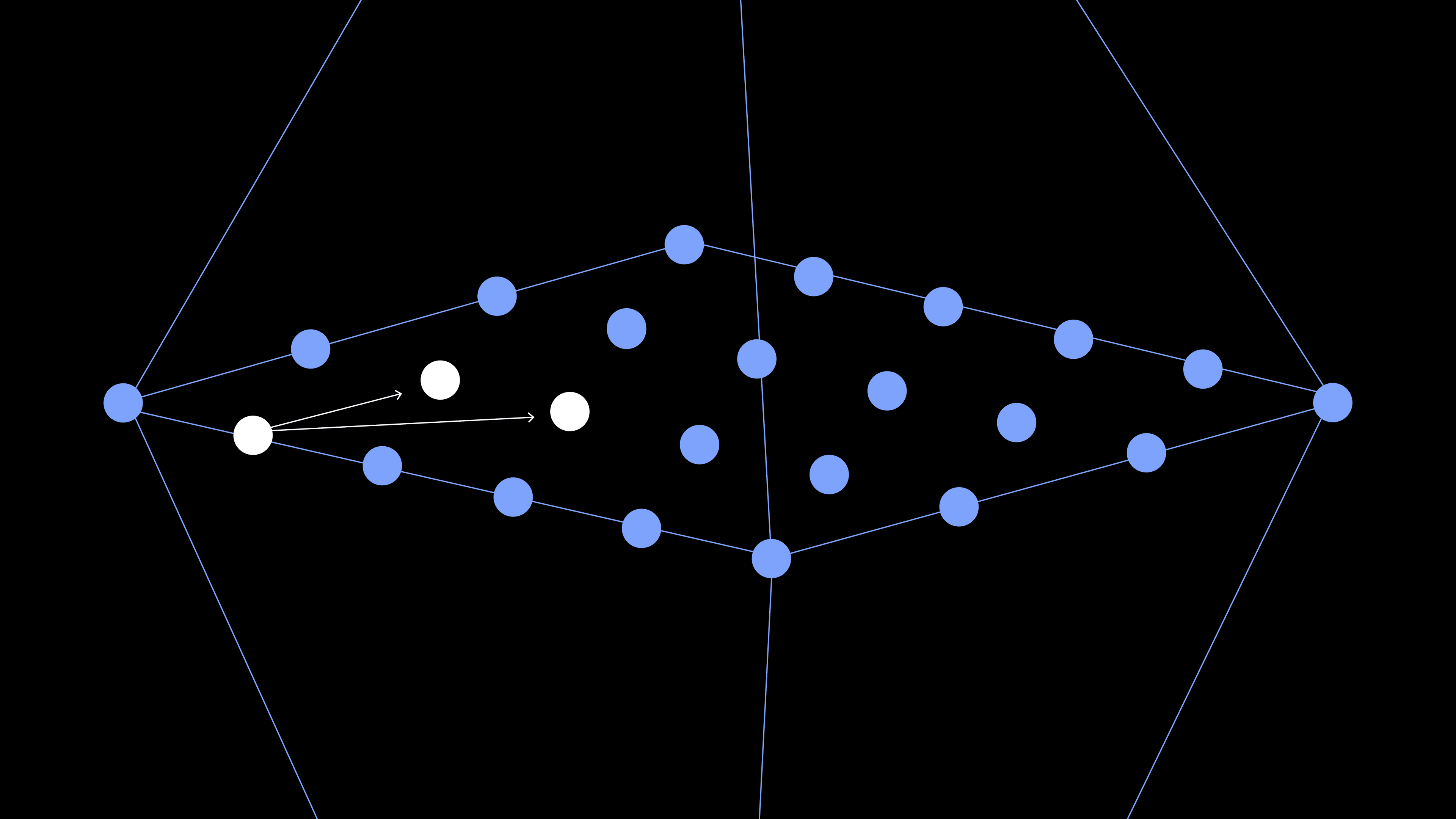
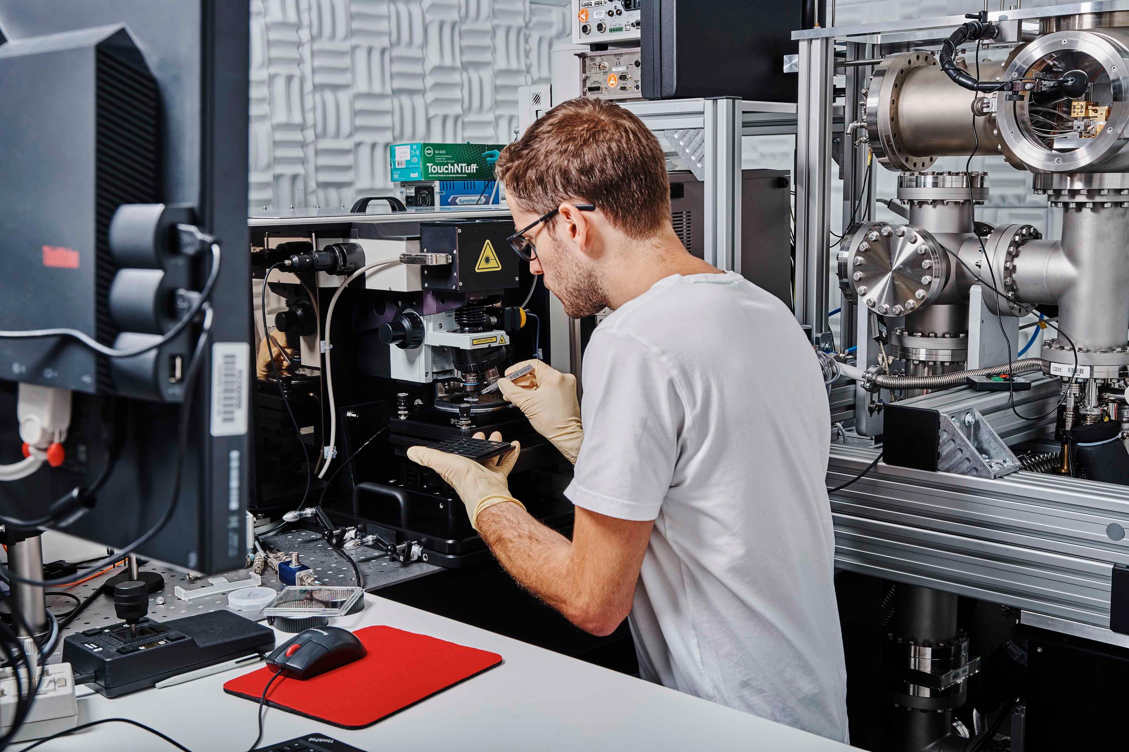
We are creating technologies that aim to seamlessly, and inherently, protect classical and next generation computing systems and allow them to stay ahead of attackers. We are designing and implementing worldwide leading innovations of the next generation of cryptography, hardware powered security, robustness of AI against adversarial attacks, decentralized trust systems (incl. Central Bank Digital Currencies), as well as system and software security analysis.
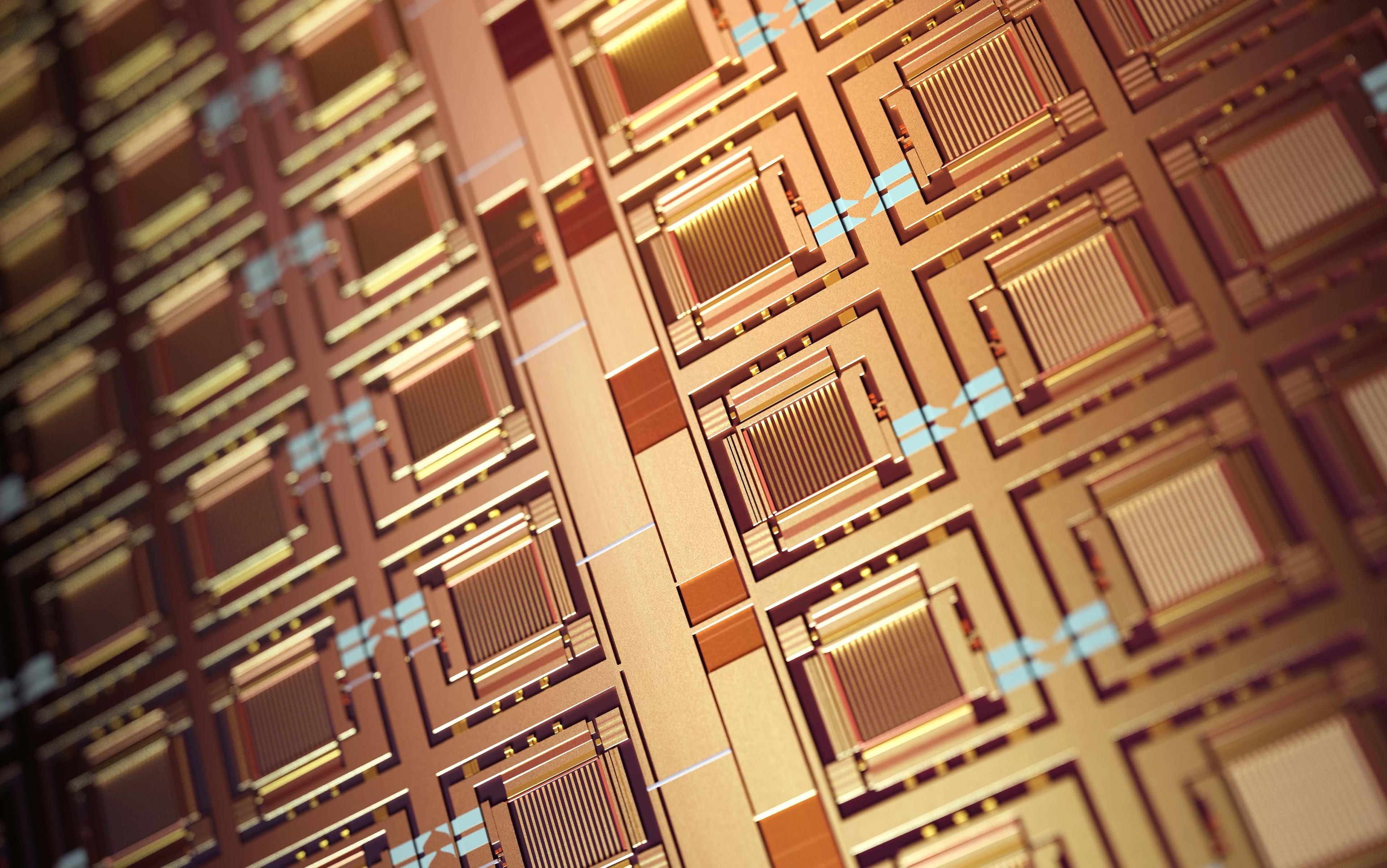
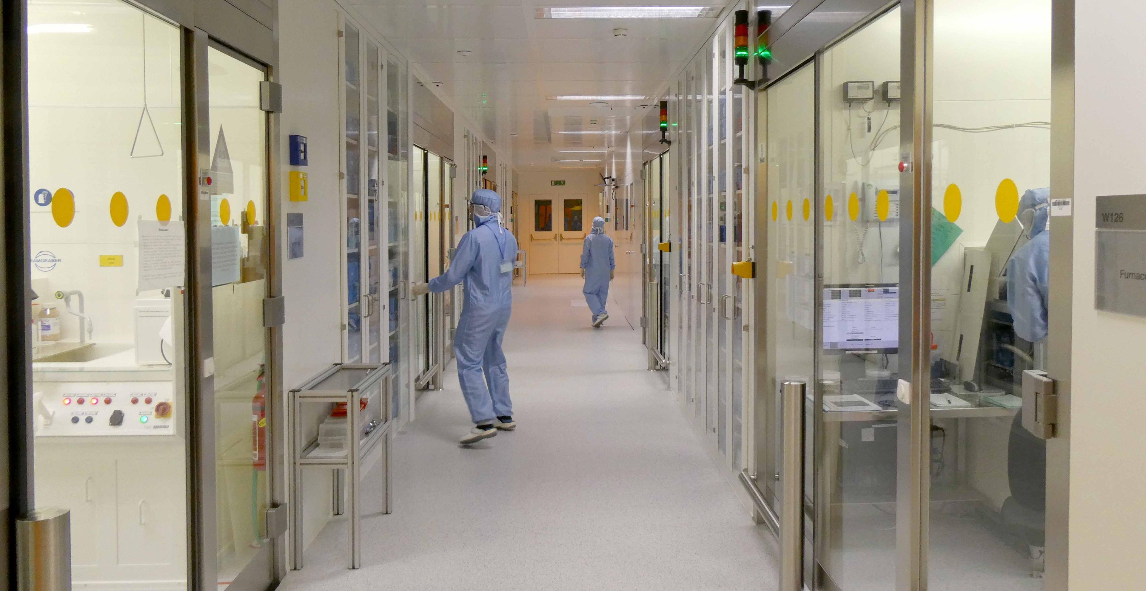
The Binnig and Rohrer Nanotechnology Center provides a cutting-edge, collaborative infrastructure designed specifically for advancing nanoscience. It hosts cleanroom space, which is jointly operated with ETH Zurich, as well as offices and dry labs. Additionally, six noise-free labs designed by IBM provide a new level of accuracy for fabricating and characterizing at the true 1-nanometer level and beyond.
We’re always looking for people excited to make a difference. See what open positions we have here and help us invent what’s next.