Nanoscale thermal phenomena are explored for applications in nanoelectronics and energy conversion. These include conventional and unconventional nanoscale devices, neuromorphic devices, molecular electronics and thermoelectricity. We aim to explore the engineering and physics of thermal processes at the nanoscale need to be explored in detail to take full advantage of the rich phenomena and to design thermal devices. The metrology associated with thermal transport at the nanoscale requires sophisticated tools and methods. Our experimental setups benefit from an optimal lab environment inside IBM’s noisefree labs.
“High-resolution thermometry techniques are essential for understanding local thermal non-equilibrium processes in many scaled devices for logic, storage and energy conversion.”
—IBM scientist Bernd Gotsmann
Research focus areas
Thermometry
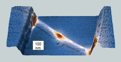
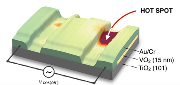
Imaging temperature fields at the nanoscale is a central challenge in various areas of science and technology. Nanoscopic hot spots, such as those observed in integrated circuits or plasmonic nanostructures, can locally modify the properties of matter, govern physical processes, and activate chemical reactions.
Specifically, future transistors are expected to be subject to serious self-heating problems. In these devices, heat has to be dissipated across many interfaces of dissimilar materials, such as semiconductors, metals and oxides. As thermal impedance mismatches between adjacent materials and confined geometries (thin films, nanowires) limit thermal transport, device-level thermal design has become necessary.
We have developed temperature mapping techniques based on scanning thermal microscopy to measure the self-heating of nanodevices with resolutions in the nanometer regime.
Webinar
Introducing the thermometry method developed at IBM Research
Research scientist Fabian Koenemann explains the thermometry method in the context of work done on the EU H2020 project CONNECT
Heat transport
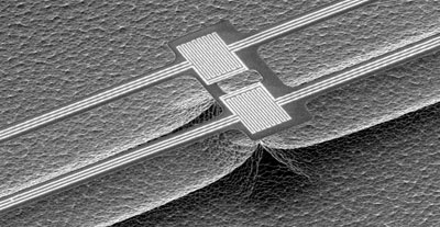
At the nanoscale, heat transport is strongly influenced by boundaries, interfaces and contacts. Nanostructured and molecular materials have specific thermal transport properties, which can be tuned for various applications. We study thermal conductance through nanoscale mechanical contacts, through molecules or vacuum gaps using scanning thermal microscopy, and through nanowire devices using MEMS-based sensors.
[ More ]
We use MEMS-based sensors to measure the thermal transport through micro-and nanoscale materials such as nanowires, nanotubes or micro-ribbons.
[ More ]
Materials & devices
Energy conversion processes between heat and electricity are at the heart of electricity generation and energy harvesting and of heat dissipation in electronic devices and cooling. We are exploring thermoelectric energy conversion in semiconducting nanostructures, pyroelectricity and electro-thermal effects in self-heated nanodevices.
Evidence of mixed axial-gravitational anomaly in thermo-electric transport in the Weyl semimetal NbP
Weyl semimetals are materials where electrons behave effectively as a kind of massless relativistic particles known as Weyl fermions. These particles occur in two flavors, or chiralities, and are subject to quantum anomalies, the breaking of a conservation law by quantum fluctuations. For instance, the number of Weyl fermions of each chirality is not independently conserved in parallel electric and magnetic field, a phenomenon known as the chiral anomaly. In addition, an underlying curved spacetime provides a distinct contribution to a chiral imbalance, an effect known as the mixed axial-gravitational anomaly, which remains experimentally elusive. However, the presence of a mixed gauge-gravitational anomaly has recently been tied to thermoelectrical transport in a magnetic field, even in flat spacetime, opening the door to experimentally probe such type of anomalies in Weyl semimetals. Using a temperature gradient, we experimentally observe a positive longitudinal magnetothermoelectric conductance (PMTC) in the Weyl semimetal NbP for collinear temperature gradients and magnetic fields (rT kB) that vanishes in the ultra quantum limit. This observation is consistent with the presence of a mixed axial-gravitational anomaly.
[ More ]
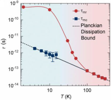
Transport at the Planckian bound of dissipation
We observed signatures of hydrodynamic electron flow in the Weyl semimetal tungsten diphosphide (WP2). Using thermal and magneto-electric transport experiments, we find indications of the transition from a conventional metallic state at higher temperatures to a hydrodynamic electron fluid below 20 K. The hydrodynamic regime is characterized by a viscosity-induced dependence of the electrical resistivity on the square of the channel width and by a strong violation of the Wiedemann–Franz law. From magneto-hydrodynamic experiments and complementary Hall measurements, the relaxation times for momentum relaxing and conserving processes are extracted. Following the uncertainty principle, both electrical and thermal transport are limited by the Planckian bound of dissipation, independent of the underlying transport regime.
[ More ]
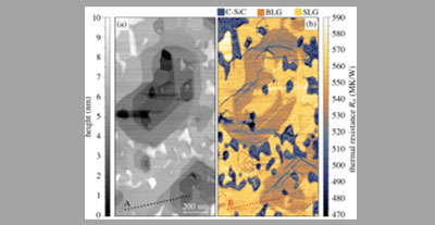
Local thermometry of self-heated nanoscale devices
Hot spots with dimensions of only a few nanometers form in numerous nanoelectronic devices. Based on recent advances in spatial resolution, these hotspots can now be studied by means of Scanning Thermal Microscopy (SThM). Here, we discuss SThM for nanoscale thermometry in comparison with other established thermometry techniques. In situ measurements of semiconductor channels for logic, and phase change memory devices are used to demonstrate today’s measurement capabilities. Temperature fields characterize not only energy dissipation in intact devices but can also serve to identify device failure and fabrication issues.
[ More ]
Ask the experts


Publications
[1] “Combined scanning probe electronic and thermal characterization of an indium arsenide nanowire”
Tino Wagner et al.
Beilstein J. Nanotechnol. 9, 129-136, 2018.
[2] “Electrical and Thermal Transport at the Planckian Bound of Dissipation in the Hydrodynamic Electron Fluid of WP2”
J. Gooth et al.
arXiv:1706.05925, 2017.
[3] “Experimental signatures of the mixed axial-gravitational anomaly in the Weyl semimetal NbP”
J. Gooth et al.
arXiv:1703.10682, 2017.
[4] “Heat transport through atomic contacts”
N. Mosso et al.
Nature Nanotechnology 72, 430-433, 2017.
[5] “A Survey of Carbon Nanotube Interconnects for Energy Efficient Integrated Circuits”
A. Todri-Sanial et al.
IEEE Circuits and Systems Magazine 17(2), 47-62, 2017.
[6] “Local thermometry of self-heated nanoscale devices”
F. Menges et al.
In Proc. IEEE International Electron Devices Meeting (IEDM), pp. 15-8, 2016.
[7] “Ballistic transport and high thermopower in one-dimensional InAs nanowires”
S. Karg et al.
In Proc. 46th European Solid-State Device Research Conference (ESSDERC), pp. 341-344, 2016.
[8] “Thermoelectric Power Factor Enhancement by Spin-Polarized Currents. A Nanowire Case Study”
A.C. Niemann et al.
Advanced Electronic Materials 2(9), 2016.
[9] “Thermal radiative near field transport between vanadium dioxide and silicon oxide across the metal insulator transition”
F. Menges et al.
Applied Physics Letters 108(17), 171904, 2016.
[10] “Temperature mapping of operating nanoscale devices by scanning probe thermometry”
F. Menges et al.
Nature Communications 7(10874), 2016.
[11] “Nanoscale thermometry by scanning thermal microscopy”
F. Menges et al.
Review of Scientific Instruments 87(7), 074902, 2016.
[12] “One-dimensional behavior and high thermoelectric power factor in thin indium arsenide nanowires”
P. Mensch et al.
Appl. Phys. Lett. 106, 093101, 2015.
[13] “Length-Dependent Thermal Transport along Molecular Chains”
T. Meier et al.
Phys. Rev. Lett. 113(6), 060801, 2014.
[14] “Full thermoelectric characterization of InAs nanowires using MEMS heater/sensors”
S.F. Karg et al.
Nanotechnology 25(30), 305702, 2014.
[15] “Using the Seebeck coefficient to determine charge carrier concentration, mobility, and relaxation time in InAs nanowires”
V. Schmidt et al.
Appl. Phys. Lett. 104, 012113, 2014.
[16] “Electrical and thermoelectrical properties of gated InAs nanowires”
P. Mensch et al.
In Proc. of European Solid-State Device Research Conference (ESSDERC), pp. 252-255, 2013.
[17] “Measurement of Thermoelectric Properties of Single Semiconductor Nanowires”
S. Karg et al.
Journal of Electronic Materials 42, 2409, 2013.
[18] “Heat dissipation and thermometry in nanosystems: When interfaces dominate”
B. Gotsmann et al.
In Proc. 71st Annual Device Research Conference (DRC), pp. 231-232, 2013.
[19] “Quantitative Thermometry of Nanoscale Hot Spots”
F. Menges et al.
Nano Letters 12(2), 596-601, 2012.
Projects and funding


EFINED
Energy Filtering Non-Equilibrium Devices

CarbON Nanotube compositE InterconneCTs

MOLESCO
Molecular-Scale Electronics

QUIET
QUalifying and Implementing a user-centric designed and EfficienT electric vehicle

Nanoheat: Multidomain Platform for Integrated More-than-Moore/Beyond CMOS Systems Characterisation & Diagnostics