One-dimensional electron system & nanoscale thermoelectrics
Continued scaling, the introduction of non-planar CMOS transistors (FinFET, Gate-all-around FET, nanowire FET) and the changeover to high-mobility channel materials will ultimately lead to noticeable quantum size effects in device characteristics.
We are investigating the transition from three-dimensional (3D) to one-dimensional (1D) electronic transport in III–V semiconductor nanowires. Moreover, we aim to improve thermoelectric devices by exploiting the unique electronic and thermal properties of semiconducting nanowires.
We are focusing on advancing our fundamental understanding of thermoelectric on the nanoscale, developing test structures for the precise measurement of relevant parameters and fabricating nanowire-based device structures with enhanced performance.
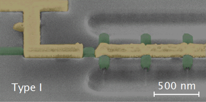
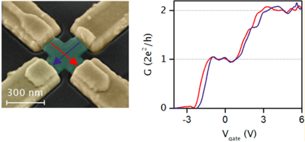
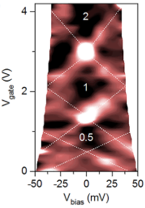
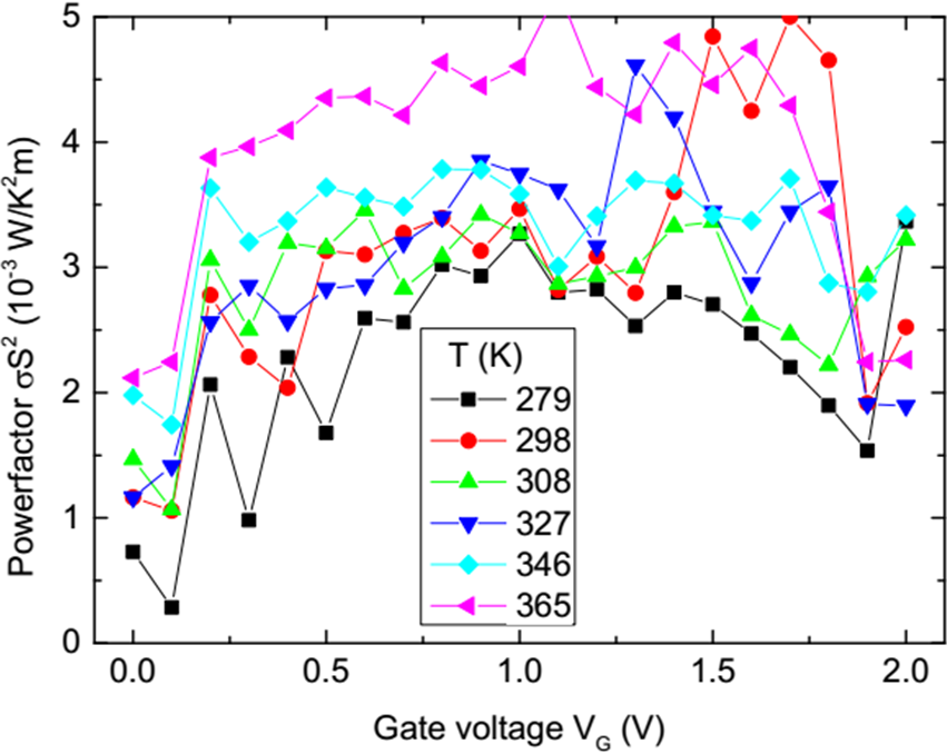
One-dimensional quantum transport across multiple nanowire junctions.
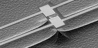
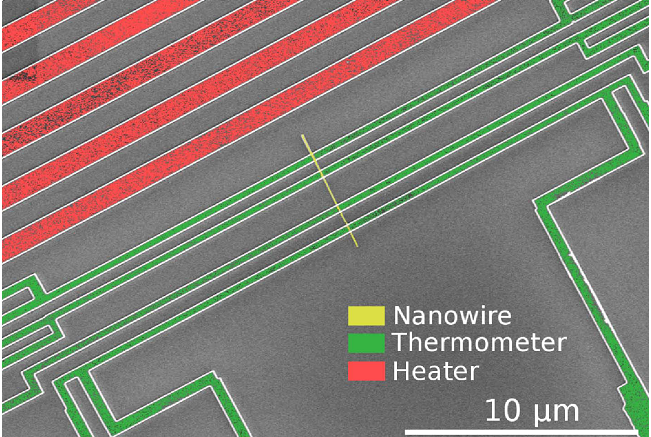
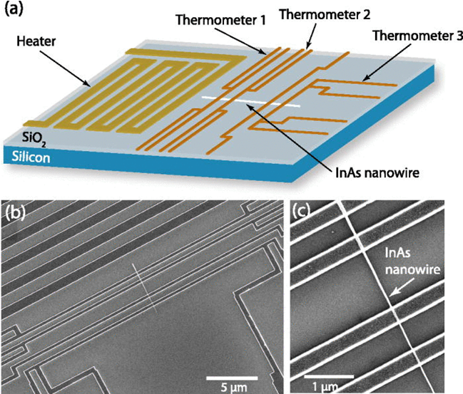
MEMS platform for thermoelectric characterization of nanowires.
Highlights
“Ballistic one-dimensional InAs nanowire cross-junction interconnects,”
J. Gooth et al.,
Nano Lett. 17(4) 2596-2602 (2017).
[ More ]
“Ballistic one-dimensional transport in InAs nanowires integrated on silicon,”
J. Gooth et al.,
Appl. Phys. Lett. 110, 083105 (2017).
[ More ]
“Ballistic transport and high thermopower in one-dimensional InAs nanowires,”
S. Karg et al.,
Solid-State Device Research Conference “ESSDERC” (2016).
[ More ]
“Temperature mapping of operating nanoscale devices by scanning probe thermometry,”
F. Menges et al.,
Nature Communications 7 (2016).
[ More ]
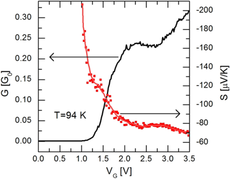
“Electrical and thermoelectrical properties of gated InAs nanowires,”
P. Mensch et al.,
Solid-State Device Research Conference “ESSDERC” (2013).
[ More ]
“Using the Seebeck coefficient to determine charge carrier concentration, mobility, and relaxation time in InAs nanowires,”
V. Schmidt et al.,
Applied Physics Letters 104, 012113 (2014).
[ More ]

“Full thermoelectric characterization of InAs nanowires using MEMS heater/sensors,”
S.F. Karg et al.,
Nanotechnology 25(30), 305702 (2014).
[ More ]

“Measurement of thermoelectric properties of single semiconductor nanowires,”
S. Karg et al.,
J. Electron. Mater. 42(7) 2409-2414 (2013).
[ More ]


