High-performance microprocessors are massively employed in data center and telecommunication infrastructures, as well as for end-use electronic devices such as laptops, smartphones and TVs. The total ICT energy consumption is estimated to be approaching 10% of the word’s electricity production. In this context, a significant amount of energy can be saved by simply improving the efficiency of microprocessors’ voltage regulator modules (VRMs).
As predicted by Moore’s Law, reducing the gate length of CMOS transistors has massively increased the data processing performance of microprocessors. However, voltage scaling in the latest nodes has deviated from Dennard’s scaling law and, hence, the power density is increasing. Modern high-performance multi-core microprocessors have power ratings of more than 100 W and feature short channel transistors with less than 1 V breakdown voltage. They require accurately regulated supply voltages even in the events of fast load changes, which occur frequently, for example if energy savings are achieved by exploiting per-core dynamic voltage and frequency scaling (DVFS). This strategy requires real-time power management and point-of-load (PoL) power converters to provide granular voltage domains depending on the load demand of each specific core or parts of a core (Figure 1).
The traditional approach uses VRMs made up of discrete components soldered on the motherboard. This provides all the necessary low voltage domains for the microprocessor. This approach results in low VRM power density, high microprocessor package input currents and, consequently, a large usage of the microprocessor’s motherboard area and package pins.
VRMs built fully on-chip or with a combination of components on-chip and on-package are usually denoted fully integrated voltage regulators (FIVRs) and use a single high-voltage domain (normally higher than the transistors’ short channel device breakdown voltage available in the chip technology node) to provide all the required voltage domains to the microprocessor. The FIVRs reduce conduction losses in the PCB and interconnects, simplify and reduce the cost the motherboard, and improve the FIVRs’ transient responses due to output load and reference voltage changes.
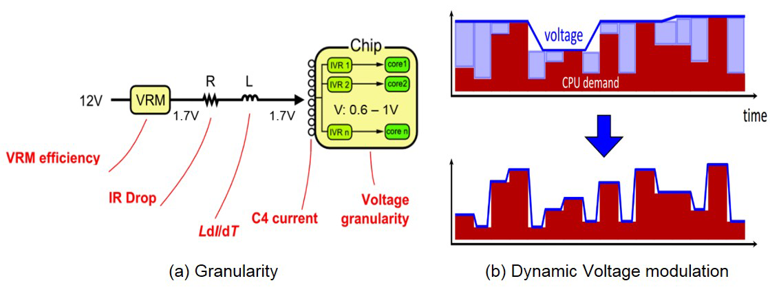
Figure 1: Schematic views depicting voltage regulation strategies to improve system efficiency. (a) Granular power delivery scheme. (b) Dynamic frequency and voltage modulation, depending on the workload.
FIVRs are found in the literature in different levels of integration relating the location of passive and active power components with respect to the microprocessor’s die: 2-D, 2.5-D, and 3-D. 2.5-D FIVRs differ from 2-D and 3-D structures in that their power components are split, the power switches are integrated onto the microprocessor’s die, and the passives are off-chip (discrete components, embedded into the package or in a silicon interposer (Figure 2a) [1]. Therefore, 2.5D integration, similar to 2D, only requires one active semiconductor die and, in addition, allows the use of passive components with lower losses at the same footprint size and reduces the expensive silicon area utilized for power management in the microprocessor’s die [2]. Using the highly efficient deep-submicron transistors in a stacked configuration (Figure 2b) allows operation at switching frequencies greater than 100 MHz and at twice the transistor’s breakdown voltage. The interleaving technique reduces the passives’ size at the input and output of the converter (Figure 2c).
![a) 2.5D FIVR with both the active components and the load realized in the same die, i.e. the chip; the passive components are built into a separate silicon interposer [3]. b) Four-phase interleaved buck converter with stacked transistors to allow operation with input voltages of up to twice the breakdown voltage of a single 32-nm transistor. c) General waveforms of the ideal four-phase buck converter for interleaved operation.](/images/st/electronicpackaging/Fig4-2.gif)
Figure 2: (a) 2.5D FIVR with both the active components and the load realized in the same die, i.e. the chip; the passive components are built into a separate silicon interposer [3]. (b) Four-phase interleaved buck converter with stacked transistors to allow operation with input voltages of up to twice the breakdown voltage of a single 32-nm transistor. (c) General waveforms of the ideal four-phase buck converter for interleaved operation.
The high number of design variables and the stringent requirements of conversion efficiency, power density, and dynamics [5] require multi-objective optimization algorithms. The Pareto-optimization procedure, successfully employed in power-management applications [3], identifies the performance limitation dictated by these technologies and allows the selection of optimal designs [4].
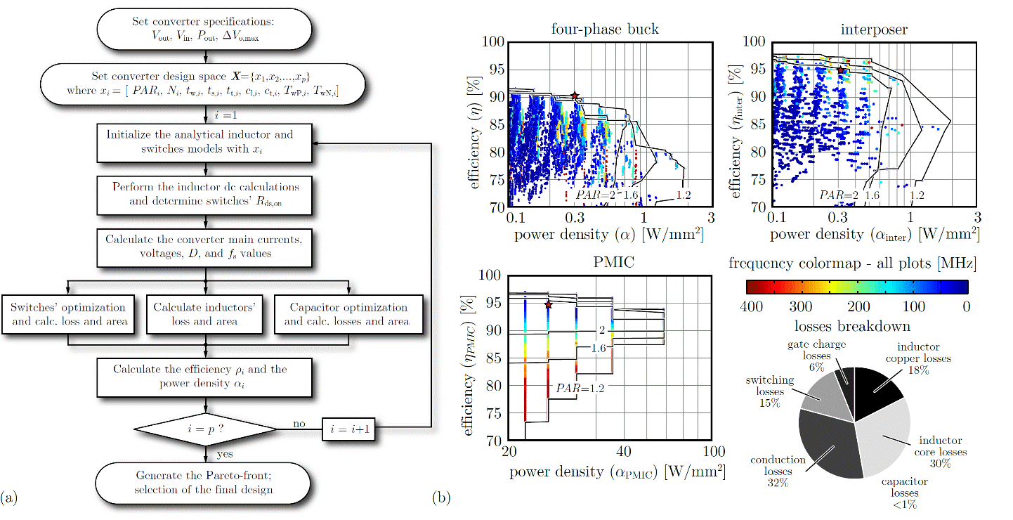
Figure 3: Multi-objective optimization of the four-phase buck converter. (a) Flowchart of the optimization algorithm. (b) Plots of the efficiency vs. power density Pareto fronts that result from the power management IC (PMIC), the interposer, and the complete four-phase buck converter. Loss breakdowns are calculated for the selected Pareto optimal design. The Pareto fronts show that either high efficiencies or high power densities are achievable with the technologies of passive and active devices [3].
References
[1] T. Andersen, P. A. M. Bezerra, F. Krismer, J. W. Kolar, A. Sridhar, T. Brunschwiler, T. Toifl, C. Rabot, Z. Pavlovic, C. O’Mathuna, S. Gaborieau, C. Bunel, “CarrICool: Interposer supporting optical signaling, liquid cooling, and power conversion for 3D chip stacks,” Proc. 4th International Power Supply on Chip Workshop (PwrSoC 2014), Boston, MA, USA, 2014.
[2] A. Sridhar, T. Brunschwiler, T. Toifl, R. Christen and J. Smajic, “Exploration of inductor-based hybrid integrated voltage regulator architectures,” Proc. 6th Electronic System-Integration Technology Conference (ESTC), Grenoble, France, pp. 1-6, 2016.
[3] P. A. M. Bezerra, T. Andersen, F. Krismer, J. W. Kolar, “Multi-objective Optimization of Fully Integrated Voltage Regulators: Switched Capacitor and Inductor-Based Converters,” ECPE PowerSoC Workshop (μPE: Powering Low-Power Systems), Ismaning/Munich, Germany, 2015.
[4] P. A. M. Bezerra et al., “Modeling and multi-objective optimization of 2.5D inductor-based Fully Integrated Voltage Regulators for microprocessor applications,” 2015 IEEE 13th Brazilian Power Electronics Conference and 1st Southern Power Electronics Conference (COBEP/SPEC), Fortaleza, pp. 1-6, 2015.
[5] R. K. Aljameh, P. A. M. Bezerra, F. Krismer, J. W. Kolar, A. Sridhar, T. Brunschwiler, T. Toifl, B. Michel, “Control and implementation aspects of a multiphase inductor-based FIVR in 14 nm bulk CMOS for microprocessor applications,” Proc. 5th International Workshop on Power Supply On Chip (PwrSoC2016), Madrid, Spain, October 3-5, 2016.
Ask the experts

Pedro Andre Martins Bezerra
IBM Research contractor

Thomas Brunschwiler
IBM Research scientist
Related projects

CarrICool
Modular interposer architecture providing scalable heat removal, power delivery and communication

ICECool
Intrachip/Interchip enhanced cooling
GaNonCMOS
GaN densily integrated with Si-CMOS for reliable, cost effective high frequency power delivery systems