Electro-thermal topologies
Electrical and thermal functionalities are typically spatially separated in current electronic packages, despite the fact that electrically conductive materials are also excellent thermal conductors. Accordingly, using a single component for electrical and thermal purposes should be considered in order to achieve more compact electronic packages. Two examples are mentioned below.
Thermal power plane (TPP)
“Using a single component for electrical and thermal purposes achieves more compact electronic packages.”
—IBM scientist Stephan Paredes
The thermal enhancement of a laminate (called TPP) with electrical power delivery capabilities enables dual-side electrical interconnects to a chip stack and thus enhances communication bandwidth and power density [1,2]. In addition, in a two-die stack, all through-silicon vias for power can be eliminated. This saves space on the silicon active area in the bottom die. The use of two laminates also allows individual testing and burn-in of the dies prior to stack formation (Figure 1).
The TPP must provide efficient heat removal and current feed in the out-of-plane and in-plane directions, respectively. We designed and implemented an 8+1 coreless buildup laminate with aligned and stacked thermal laminate vias (TLVs). Rail-shaped solder interconnects join the TPP to the top of the chip stack, achieving better heat dissipation capabilities than solder balls. In principle, the solder interface and the TPP with their thermal impedances of 4.8 and 7.4 K mm2 W−1, respectively, represent an electrically functional TIM1 and lid with a performance equivalent to that of electrical non-functional TIMs and lids used in state-of-the-art packages (Figure 2).
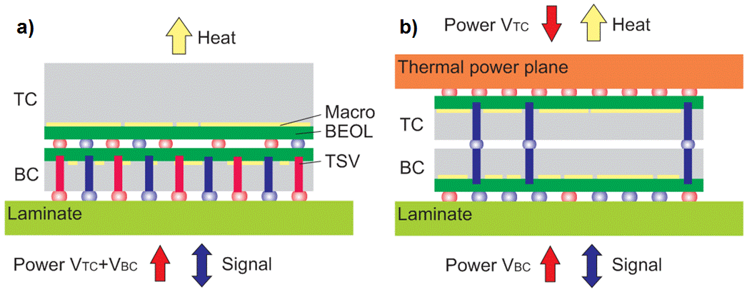
Figure 1: Cross-sectional view of a module with a two-die chip stack. a) Single-side electrical interconnects, b) dual-side electrical interconnects (red: power, blue: signals, yellow: heat).
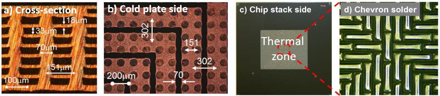
Figure 2: Photographs of a TPP with chevron design and solder rails: Micrographs depicting TPP a) cross section and b) top side. c) Bottom view of the entire TPP laminate (50×50 mm2). d) Close-up of the solder rail array with rail length and width of 900×250 μm2.
Thermal-power insert
A dual-side cooling topology can be achieved by embedding a thermal-power insert into the organic substrate of a chip or chip stack (Figures 3 and 4). The thermal-power (TP) insert consist of laminated copper sheets embedded into the substrate. The copper sheets are oriented perpendicular to the substrate surface and provide a direct conduction path for heat and current in and out of plane, with a copper fill fraction of up to 90%. Additional lamination layers on-top of the TP insert can provide redistribution wiring if required.
The resulting substrate topology respects the high-density fan-out of signals from the periphery of the chip and the high currents to be provided to the chip center area. From a thermal perspective, the substrate represents an electrically active lid, with the solder interconnects serving as TIM1. Rail-like solder shapes were proposed to improve the thermal contact to the substrate fourfold compared to solder ball arrays [3].
As a result, the thermal impedance from the chip or chip stack to the top and the bottom cold plate can be equivalent, considering the TP insert concept. Accordingly, either the power density of a chip can be doubled for the given thermal budget or the temperature gradient can be halved at a fixed power density. Dual-side cooling will also enable the integration of high-power dies in the bottom layers of a chip stack, providing a direct heat removal path without the dissipation through all the thermal interfaces from within the chip stack.
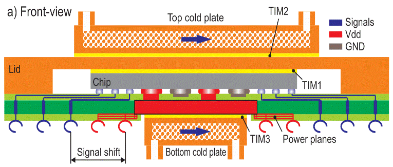
Figure 3: a) Front and b) side view of the dual-side cooling topology enabled by the thermal-power insert. Note that in b), the cold plates, lid and TIMs were omitted for clarity.
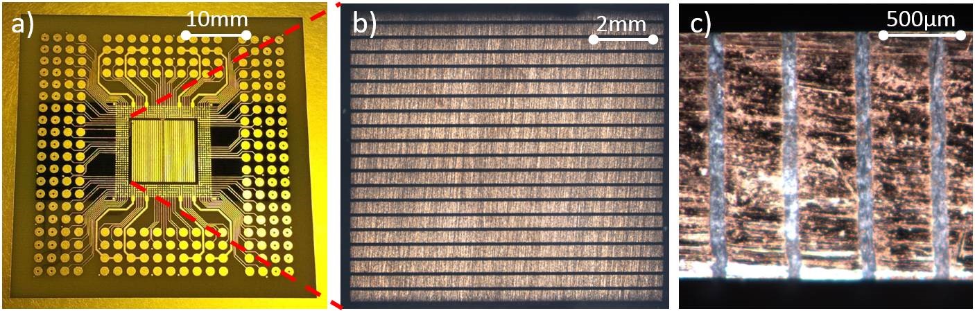
Figure 4: a) Photograph of a substrate with an embedded TP insert. Micrographs depicting the TP insert before embedding in a) top and b) side view.
References
[1] T. Brunschwiler, R. Heller, G. Schlottig, T. Tick, H. Harrer, H. Barowski, T. Niggemeier, J. Supper, and S. Oggioni, “Thermal Power Plane enabling Dual-Side Electrical Interconnects for High-Performance Chip Stacks: Concept,’ ESTC, Helsinki, Finnland, 2014.
[2] T. Brunschwiler, T. Tick, M. Castriotta, G. Schlottig, D. Gschwend, K. Sato, T. Nakajima, S. Li, and S. Oggioni, “Thermal Power Plane enabling Dual-Side Electrical Interconnects for High-Performance Chip Stacks: Implementation,’ ESTC, Helsinki, Finnland, 2014.
[3] T. Brunschwiler, D. Gschwend, S. Paredes, T. Tick, K. Matsumoto, Ch. Lehnberger, J. Pohl, U. Zschenderlein and S. Oggioni, “Embedded Power Insert Enabling Dual-Side Cooling of Microprocessors,” Proceedings of ECTC, San Diego, CA, 2015.
Ask the experts

Stefano Oggioni
IBM Systems

Stephan Paredes
IBM Research scientist

Thomas Brunschwiler
IBM Research scientist